Part Number: ADS1298
Tool/software:
Hi all,
I am trying to work with an ADS1298 board I inherited by first trying to read the ID of the board before trying to read ECG data. Since it's an ADS1298, I'm expecting the message 0x92, but I am not reading any data on the DOUT line (MISO). I checked the FAQ section for this chip and nothing really helped. I followed the power up sequence guide and VCAP1 seems to be above 1.1V at around 1.3V, so something must go wrong after this step.
I am using a NUCLEO STM32F767ZI for communicating with the ADS chip. In the screenshot below you can see the two functions I used to power up the chip and initialize it for reading the ID. The first one is running only once, and the second one is running continuously.
void ADS1298_Init(SPI_HandleTypeDef *hspi)
{
uint8_t wakeupCmd = 0x02; // Wakeup command
uint8_t rregCmd = 0x11; // SDATAC mode command for sending data
uint8_t resetCmd = 0x06; // Reset command
HAL_GPIO_WritePin(GPIOA, GPIO_PIN_4, GPIO_PIN_RESET); //PA4 is custom set as SPI1_CS - set now LOW because of the transaction start
HAL_GPIO_WritePin(GPIOA, GPIO_PIN_5, GPIO_PIN_RESET); //START pin starts LOW - PA5 -- TRY THIS, according to the datasheet DRDY is supposed to toggle at tclk/8192 after this step?
HAL_GPIO_WritePin(GPIOA, GPIO_PIN_6, GPIO_PIN_SET); // The default state of the PWDN pin is high - set HIGH
HAL_GPIO_WritePin(GPIOA, GPIO_PIN_3, GPIO_PIN_SET); // The default state of the RESET pin is high - set HIGH
HAL_Delay(100);
HAL_GPIO_WritePin(GPIOA, GPIO_PIN_3, GPIO_PIN_RESET); // RESET set LOW
HAL_Delay(100);
HAL_GPIO_WritePin(GPIOA, GPIO_PIN_3, GPIO_PIN_SET); // RESET set HIGH
HAL_Delay(100); //The last 3 blocks of code changing RESET make up the power-up sequence
HAL_SPI_Transmit(&hspi1, &wakeupCmd, 1, HAL_MAX_DELAY); //Wake up from standby mode
HAL_Delay(1);
transferSPI(resetCmd); // Reset command
//HAL_SPI_TransmitReceive(&hspi1, &resetCmd, 1, HAL_MAX_DELAY); // Send the RESET command -- OR THIS, how I did the line above before
HAL_GPIO_WritePin(GPIOA, GPIO_PIN_4, GPIO_PIN_SET); // Setting CS high again
HAL_Delay(500);
HAL_GPIO_WritePin(GPIOA, GPIO_PIN_4, GPIO_PIN_RESET);
transferSPI(rregCmd); // SDATAC command, stop reading data so the ADS1298 can receive commands
HAL_GPIO_WritePin(GPIOA, GPIO_PIN_4, GPIO_PIN_SET);
HAL_Delay(500);
}
void ADS1298_SendID(SPI_HandleTypeDef *hspi)
{
uint8_t command[2]; //Buffer for sending commands to the ADS1298
uint8_t rregCmd = 0x11; // SDATAC mode command for sending data
HAL_GPIO_WritePin(GPIOA, GPIO_PIN_4, GPIO_PIN_RESET);
transferSPI(rregCmd); // SDATAC command, stop reading data so the ADS1298 can receive commands
command[0] = 0x20 | 0x00; // RREG opcode command reads register data from the 0x00 address (ID register)
command[1] = 0x00; // Number of registers to read - 1 (only 1 register)
HAL_SPI_Transmit(&hspi1, command, sizeof(command), HAL_MAX_DELAY); // Send the RREG command
//transferSPI(command); // OR THIS - but it doesn't seem like it is working
//HAL_Delay(1);
HAL_SPI_Receive(&hspi1, response, sizeof(response), HAL_MAX_DELAY); // Read the ID register value
//HAL_Delay(1);
// Pull CS high to deselect the ADS1298
HAL_GPIO_WritePin(GPIOA, GPIO_PIN_4, GPIO_PIN_SET);
}
These are the SPI settings (SCLK is at 3 MHz):
static void MX_SPI1_Init(void)
{
/* USER CODE BEGIN SPI1_Init 0 */
/* USER CODE END SPI1_Init 0 */
/* USER CODE BEGIN SPI1_Init 1 */
/* USER CODE END SPI1_Init 1 */
/* SPI1 parameter configuration*/
hspi1.Instance = SPI1;
hspi1.Init.Mode = SPI_MODE_MASTER;
hspi1.Init.Direction = SPI_DIRECTION_2LINES;
hspi1.Init.DataSize = SPI_DATASIZE_8BIT;
hspi1.Init.CLKPolarity = SPI_POLARITY_LOW;
hspi1.Init.CLKPhase = SPI_PHASE_2EDGE;
hspi1.Init.NSS = SPI_NSS_SOFT;
hspi1.Init.BaudRatePrescaler = SPI_BAUDRATEPRESCALER_32;
hspi1.Init.FirstBit = SPI_FIRSTBIT_MSB;
hspi1.Init.TIMode = SPI_TIMODE_DISABLE;
hspi1.Init.CRCCalculation = SPI_CRCCALCULATION_DISABLE;
hspi1.Init.CRCPolynomial = 7;
hspi1.Init.CRCLength = SPI_CRC_LENGTH_DATASIZE;
hspi1.Init.NSSPMode = SPI_NSS_PULSE_DISABLE;
if (HAL_SPI_Init(&hspi1) != HAL_OK)
{
Error_Handler();
}
/* USER CODE BEGIN SPI1_Init 2 */
/* USER CODE END SPI1_Init 2 */
}
Some relevant info that cannot be seen in the screenshot I took on the oscilloscope: the DRDY pin is stuck high. I am using a custom GPIO pin for CS, will report back later if I'm facing the same issue with the NSS pin for SPI1. I have also seen some people setting up the DRDY pin as an interrupt, will also do that and report later, but I doubt this is the main problem since I am not reading anything on the MISO line.
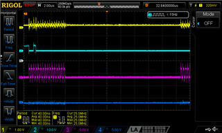
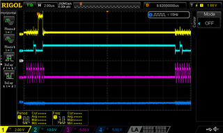
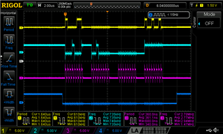
Below you can see a screenshot from the oscilloscope of the SPI communication. From top to bottom, the lines are MISO, MOSI, CLK and CS. Any help would be greatly appreciated!