ADS1298: ads1298 init and configure issues

Part Number: ADS1298

Tool/software:

Hi,

Im tring to get the ads1298 upp and running. But have some issues.

Followed the setup sequence "see code"  after setup I'm sending the SDATAC and STOP command one after each other to be able to read back registers.

Main issue is tha i cant send the first command over the SDATAC, it is not recognised by the ADS,  the SPI line is upp high and ignors the first data send and becouse of this i have to send a dumy data to get it started, any idea on this??

Im also using the START pin to control it, but it has no effect when I pull it low and start to read the register values.

void ads1298r_ctrl_init_device(void) {

	// Disable data interrupts for the ADS converter
	 HAL_NVIC_DisableIRQ(EXTI1_IRQn);

	SPI_ADS_START_ON_OFF(0);
	DELAY_MS(1);

	// Initialise ADS using RESET PIN
	ads1298r_reset_pin();
	// Reset sequence is finished

}


//-- Configure the ADS through SPI
void ads1298r_init(void) {

	//  Enabling the ADS modules
	SPI_ADS_COM_ON_OFF(0);
	//	Stopping the ADS sensor
	SPI_ADS_START_ON_OFF(0);
	DELAY_MS(1);

	// Send dumy data to be able to continue with the configuration
	ads_read_reg(0x00);

	// STOP all data transmission for configuration
	ads1298r_SDATAC();
	ads1298r_STOP();
	DELAY_MS(1);

	//	Sending out configuration data to the ECG sensors
	init_ads1298r_EPMCG_experiment_LOFF();

	// Initialise Data reception form the ADS
	// First it need to be started this function includes a command and also a START pin set to LOW
	ads1298r_RDATAC();
	ads1298r_START();
	DELAY_MS(100);

	// Re Enable the interrupts to have a breathing time for DMA
	HAL_NVIC_EnableIRQ(EXTI1_IRQn);

}
/*
 * New configuration file for the ECG ADS sensors
 */
void init_ads1298r_EPMCG_experiment_LOFF(void){

	uint8_t buffer[3];

	// Enable ECG and PMCG at the Same time
//	SPI_ADS_COM_ON_OFF(1);

	// REG CONFIG 1
	//Set Data Rate 4kHz with DEFAULT LOW-POWER mode
//	ads1298r_SetDataRate(ADS129X_SAMPLERATE_4k_64);
	// REGS - 0b0xxx xxxx - LP mode
	// REGS - 0bx1xx xxxx - Multiple readback mode
	// REGS - 0bxx0x xxxx - Oscillator clock output disabled
	// REGS - 0bxxxx x010 - Set data ready to 4kSPS
	// REGS Final - 0b0100 0010
	ADS_Transmit(ADS129X_REG_CONFIG1, 0x00, 0b01000010);

	// REG CONFIG 3
	// Enable internal reference buffer - 0_1xxxxxxx
	// SET Internal RLD signals - 0_xxxx1xxx
	// RLD buffer ENABLE - 0_xxxxx1xx

	// REG - 0x10001100
	ADS_Transmit(ADS129X_REG_CONFIG3, 0x73, ADS129X_PD_REF_ENABLED | ADS129X_RLD_REF_SIG_INTERNAL | ADS129X_RLD_BUFFER_ENABLED);

//	ADS_Transmit(ADS129X_REG_CONFIG3, 0x7F, ADS129X_PD_REF_ENABLED);
//	ADS_Transmit(ADS129X_REG_CONFIG3, 0xF7, ADS129X_RLD_REF_SIG_INTERNAL);
//	ADS_Transmit(ADS129X_REG_CONFIG3, 0xFB, ADS129X_RLD_BUFFER_ENABLED);


	// ALL GAIN and Electrode MODE set to 0x00

	// Setup channels of the ECG ADS
	// Easier if channels are set up using simple SPI transfer to ADS
	// Currently it checks the state of the register then writes in the changes
	ADS_Transmit(ADS129X_REG_CH1SET, 0xF8, ADS129X_MUX_NORMAL);
	ADS_Transmit(ADS129X_REG_CH2SET, 0xF8, ADS129X_MUX_NORMAL);
	ADS_Transmit(ADS129X_REG_CH3SET, 0xF8, ADS129X_MUX_NORMAL);
	ADS_Transmit(ADS129X_REG_CH4SET, 0xF8, ADS129X_MUX_NORMAL);
	ADS_Transmit(ADS129X_REG_CH5SET, 0xF8, ADS129X_MUX_NORMAL);
	ADS_Transmit(ADS129X_REG_CH6SET, 0xF8, ADS129X_MUX_NORMAL);
	ADS_Transmit(ADS129X_REG_CH7SET, 0xF8, ADS129X_MUX_NORMAL);
	ADS_Transmit(ADS129X_REG_CH8SET, 0xF8, ADS129X_MUX_NORMAL);

	// Channel gain settings each channel has to be written separately
	// Gain set to GAIN_6
	ADS_Transmit(ADS129X_REG_CH1SET, 0x00, ADS129X_GAIN_6X);
	ADS_Transmit(ADS129X_REG_CH2SET, 0x00, ADS129X_GAIN_6X);
	ADS_Transmit(ADS129X_REG_CH3SET, 0x00, ADS129X_GAIN_6X);
	ADS_Transmit(ADS129X_REG_CH4SET, 0x00, ADS129X_GAIN_6X);
	ADS_Transmit(ADS129X_REG_CH5SET, 0x00, ADS129X_GAIN_6X);
	ADS_Transmit(ADS129X_REG_CH6SET, 0x00, ADS129X_GAIN_6X);
	ADS_Transmit(ADS129X_REG_CH7SET, 0x00, ADS129X_GAIN_6X);
	ADS_Transmit(ADS129X_REG_CH8SET, 0x00, ADS129X_GAIN_6X);

	// Setup reference voltage to REF_2_4_V
	// Config REG - 0_xx0xxxxx
	ADS_Transmit(ADS129X_REG_CONFIG3, 0xDF, ADS129X_REF_VOLTAGE_2_4V);

	// RLD_SENSP
	// ch2 and ch3 set - 0x00000110
	// Note channels are counted from the right side - 0x87654321
	ADS_WREG(ADS129X_REG_RLD_SENSP, 0x00000110);

	// RLD_SENSN
	// ch2 set - 0x00000010 - NOT USED
	// 0x00000000 - Currently Used
	// Note channels are counted from the right side - 0x87654321
	ADS_WREG(ADS129X_REG_RLD_SENSN, 0x00000000);


	// WCT1
	// bit3 PD_WCTS = 1 poweron
	// WCTA 011, channel2 negative

	//WCT settings
	ADS_Transmit(ADS129X_REG_CONFIG3, 0xFB, ADS129X_WCTA_STAT_POWERED_DOWN);
	ADS_Transmit(ADS129X_REG_WCT1, 0xF8, ADS129X_WCTAC_AMP_CH2_N);

	// WCT2
	// PD_WCTC = 1 powered on
	// PD_WCTB = 1 powered on
	// WCTB 010
	// WCTC 100

	//WCT connection settings
	ADS_Transmit(ADS129X_REG_WCT2, 0xBF, ADS129X_WCTB_STAT_POWERED_ON);
	ADS_Transmit(ADS129X_REG_WCT2, 0xC7, ADS129X_WCTB_AMP_CH2_P);
	ADS_Transmit(ADS129X_REG_WCT2, 0x7F, ADS129X_WCTC_STAT_POWERED_ON);
	ADS_Transmit(ADS129X_REG_WCT2, 0xF8, ADS129X_WCTAC_AMP_CH3_P);


	// Lead off detection settings /--------------------------------/
	// Simple trasfer is used to write to the ADS
	// other way errors didnt let the transfer to compleate lossing the settings

	//  Register setup: 111 _ 1 _ 00 _ 11

	// 111 - Positive sied 70% , negative side 30%
	// 1 - pullup or pulldown resistor mode lead-of
	// 00 - current magnitude 6nA
	// 11 - DC lead-off detection turned on

	// Enable the lead off settings
	ADS_WREG(ADS129X_REG_LOFF, 0b11100011);

	// Turn on the lead off comparator
	// 0bxxxxxx1x - Lead-off comparators enabled
	//Configure the register to handle the lead off settings
	ADS_WREG(ADS129X_REG_CONFIG4, 0b00000010);


	// Which channels to turn on the Lead off SENSP and SENSN
	// Enable all LOFF channels for SENSP
	// Write in enable and disable to LOFF channels
	ADS_WREG(ADS129X_REG_LOFF_SENSP, 0b11111111);
	// Enable all LOFF channels for SENSN
	// Write in enable and disable to LOFF channels
	ADS_WREG(ADS129X_REG_LOFF_SENSN, 0b11111111);


//	SPI_ADS_COM_ON_OFF(0);

	//	delayUs(20);
	//Task_sleep(1);
}


// Function to start the data transfer
//void task_ads1298r_stop(void) {
	//while(true) {
	//Semaphore_pend(ads1298r_start_sem_handle, BIOS_WAIT_FOREVER);

//	ads1298r_stop();

	//}
//}

void ads1298r_RDATAC(void)
{
	// START continuous read on the ADS converter
	// Setup command for START sequence
	SPI_ADS_START_ON_OFF(0);
	DELAY_MS(1);

	// 0x10 - Data to be sent to STOP the continuouse conversion
	ads_write_command(ADS129X_CMD_RDATAC);
	DELAY_MS(1);

	// pull up the START pin
	SPI_ADS_START_ON_OFF(1);
	DELAY_MS(1);
}
/*
 *  ======== Stop ========
 *  Stop the ADS1298r device.
 */
void ads1298r_SDATAC(void)
{
	// STOP continuous read on the ADS converter
	// Setup command for STOP sequence
	SPI_ADS_START_ON_OFF(1);
	DELAY_MS(1);

	// 0x11 - Data to be sent to STOP the continuouse conversion
	ads_write_command(ADS129X_CMD_SDATAC);
	DELAY_MS(1);

	// Pull up the START pin
	SPI_ADS_START_ON_OFF(0);
	DELAY_MS(1);
}

void ads1298r_START(void)
{
	// START continuous read on the ADS converter
	// Setup command for START sequence
	SPI_ADS_START_ON_OFF(0);
	DELAY_MS(1);

	// 0x00 - Data to be sent to STOP the continuouse conversion
	ads_write_command(ADS129X_CMD_START);
	DELAY_MS(1);

	// pull up the START pin
	SPI_ADS_START_ON_OFF(1);
	DELAY_MS(1);
}

void ads1298r_STOP(void)
{
	// STOP continuous read on the ADS converter
	// Setup command for STOP sequence
	SPI_ADS_START_ON_OFF(0);
	DELAY_MS(1);
	SPI_ADS_START_ON_OFF(1);
	DELAY_MS(1);

	// 0x00 - Data to be sent to STOP the continuouse conversion
	ads_write_command(ADS129X_CMD_STOP);
	DELAY_MS(1);

	// pull up the START pin
	SPI_ADS_START_ON_OFF(0);
	DELAY_MS(1);
}

/*
 *  ======== Reset ========
 *  Reset the ADS1298r device.
 */
void ads1298r_reset_pin(void)
{
	SPI_ADS_RST_OFF_ON(1);
	DELAY_MS(200);

	// Perform a ADS reset sequence Pull RESET pin LOW
	SPI_ADS_RST_OFF_ON(0);
	DELAY_MS(10);

	SPI_ADS_RST_OFF_ON(1);
	DELAY_MS(100);

}
void ads1298r_reset_command(void)
{
	// Setup command for RESET sequence
	// 0x06 - Data to be sent to RESET the continuouse conversion
	ads_write_command(ADS129X_CMD_RESET);
//	ADS_WREG(_address, 0x00);
	HAL_Delay(10);
}


uint8_t ads1298r_read_ID(void)
{
	// 0x00 - Read Reg ID, If cant  read continue
	uint8_t timeout = 10;

	while (timeout--){

		uint8_t reg_data = ads_read_reg(ADS129X_REG_ID);

		DELAY_MS(1);

		if(reg_data == 0x92)
			return 1;

	}
}


//-- Configure the ADS through SPI - ...
void task_ads1298r_start(void){

	//	Start the Data reception from the ADS
//	ads1298r_start();
	HAL_Delay(1);

	//  Enable interrupts on the ADS DRDY PIN
//	HAL_NVIC_EnableIRQ(EXTI2_IRQn);

	HAL_Delay(4);

}

NOTE: code got updated

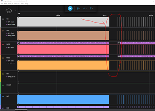
Logic analyzer picture, missing the 0x00 red-back, but afterwards the read-back starts as the analyzer shows the correct values being received by the mcu.

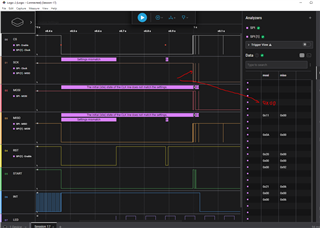
1, Any idea why this happens, am I missing something in the initialization phase ?

2, I there any example code which shows the proper initialisation sequence?

3, why does the 4k sampling rate changes back to 250Hz ?

  • Code related to SPI, if someone finds it useful.

    SPI_HandleTypeDef ads_spiHandle;
    
    GPIO_TypeDef* _csPort;
    uint16_t _csPin;
    
    GPIO_TypeDef* _startPort;
    uint16_t _startPin;
    
    GPIO_TypeDef* _rstPort;
    uint16_t _rstPin;
    
    
    void SPI_config(SPI_HandleTypeDef *spi_cls, GPIO_TypeDef* cs_port, uint16_t cs_pin) {
    	ads_spiHandle = *spi_cls;
    	_csPort = cs_port;
    	_csPin = cs_pin;
    }
    void SPI_P_config(SPI_HandleTypeDef *spi_cls) {
    	ads_spiHandle = *spi_cls;
    }
    void SPI_CS_config(GPIO_TypeDef* cs_port, uint16_t cs_pin) {
    	_csPort = cs_port;
    	_csPin = cs_pin;
    }
    
    void SPI_ADS_pin_config(GPIO_TypeDef* start_port, uint16_t start_pin, GPIO_TypeDef* rst_port, uint16_t rst_pin) {
    	_startPort = start_port;
    	_startPin = start_pin;
    	_rstPort = rst_port;
    	_rstPin = rst_pin;
    }
    
    void SPI_ADS_COM_ON_OFF(uint8_t state) {
    	if(state){
    		HAL_GPIO_WritePin(_csPort, _csPin, GPIO_PIN_RESET);
    	}
    	else{
    		HAL_GPIO_WritePin(_csPort, _csPin, GPIO_PIN_SET);
    	}
    }
    void SPI_ADS_START_ON_OFF(uint8_t state) {
    	if(state){
    		HAL_GPIO_WritePin(_startPort, _startPin, GPIO_PIN_SET);
    	}
    	else{
    		HAL_GPIO_WritePin(_startPort, _startPin, GPIO_PIN_RESET);
    	}
    }
    void SPI_ADS_RST_OFF_ON(uint8_t state) {
    	if(state){
    		HAL_GPIO_WritePin(_rstPort, _rstPin, GPIO_PIN_SET);
    	}
    	else{
    		HAL_GPIO_WritePin(_rstPort, _rstPin, GPIO_PIN_RESET);
    	}
    }
    
    
    uint8_t ads_read_reg(uint8_t reg_address){
    
    	uint8_t txData[3];
    	uint8_t rxData[3];
    
    	txData[0] = ADS129X_CMD_RREG | reg_address;
    	txData[1] = 0x00;
    	txData[2] = 0x00;
    
    
    	SPI_ADS_COM_ON_OFF(1);
    
    	HAL_SPI_TransmitReceive(&ads_spiHandle, &txData, &rxData, 3, 1);
    
    	while(HAL_SPI_GetState(&ads_spiHandle)!= HAL_SPI_STATE_READY){}
    
    	SPI_ADS_COM_ON_OFF(0);
    
    	return rxData[2];
    }
    uint8_t ads_write_reg(uint8_t reg_address, uint8_t data){
    
    	uint8_t txData[3];
    	uint8_t rxData[3];
    
    	txData[0] = ADS129X_CMD_WREG | reg_address;
    	txData[1] = 0x00;
    	txData[2] = data;
    
    
    	SPI_ADS_COM_ON_OFF(1);
    
    	HAL_SPI_Transmit(&ads_spiHandle, &txData, 3, 0);
    
    	while(HAL_SPI_GetState(&ads_spiHandle)!= HAL_SPI_STATE_READY){}
    
    	SPI_ADS_COM_ON_OFF(0);
    
    	return rxData[2];
    }
    uint8_t ads_write_command(uint8_t reg_address){
    
    	uint8_t txData[3];
    	uint8_t status;
    
    	txData[0] = reg_address;
    
    	SPI_ADS_COM_ON_OFF(1);
    
    	status = HAL_SPI_Transmit(&ads_spiHandle, &txData, 1, 0);
    
    	while(HAL_SPI_GetState(&ads_spiHandle)!= HAL_SPI_STATE_READY){}
    
    	SPI_ADS_COM_ON_OFF(0);
    
    	return status;
    }
    
    /*
     *  ======== Read ========
     *  Read data from the ADS1298r device.
     */
    void ads1298r_read(uint8_t* buffer, size_t size) {
    
    	bool transferOK;
    	uint8_t txData[size];
    
    //	transferOK = HAL_SPI_TransmitReceive(&ads_spiHandle, &txData, &buffer, size, 1);
    	transferOK = HAL_SPI_Receive(&ads_spiHandle, &buffer, size, 0x100);
    
    	if(!transferOK) {
    		//		System_printf("Unsuccessful SPI transfer");
    	}
    	//	HAL_GPIO_TogglePin(LED_INDI_GPIO_Port, LED_INDI_Pin);
    }
    
    /*
     *  ======== Transfer ========
     *  Transfer data between ADS1298r and MCU.
     */
    
    uint8_t ads1298r_transfer(uint8_t address, uint8_t* buffer, uint8_t length)
    {
    	uint8_t transferOK;
    	uint8_t errorCode = 0x00;
    
    	uint8_t add[1] = {address};
    	uint8_t len = length;
    	uint8_t *buf = buffer;
    	uint8_t tempRxBuffer[1];
    
    	uint8_t count_len;
    
    	count_len = 1;
    
    	transferOK = HAL_SPI_TransmitReceive(&ads_spiHandle, &add, &tempRxBuffer[0], count_len, 1);
    	while(HAL_SPI_GetState(&ads_spiHandle)!= HAL_SPI_STATE_READY){}
    
    	//  Check if the SPI communication is good
    	if(transferOK != HAL_SPI_STATE_READY) {
    		errorCode = 0x01;
    	}
    
    	if (length > 0) {
    		// Send length to ADS1298r
    		len = length - 1;
    		transferOK = HAL_SPI_TransmitReceive(&ads_spiHandle, &len, &tempRxBuffer[0], count_len, 1);
    		while(HAL_SPI_GetState(&ads_spiHandle)!= HAL_SPI_STATE_READY){}
    
    		//  Check if the SPI communication is good
    		if(transferOK != HAL_SPI_STATE_READY) {
    			errorCode = 0x01 << 1;
    		}
    		count_len = length;
    		// Send data to ADS1298r
    		transferOK = HAL_SPI_TransmitReceive(&ads_spiHandle, &buf, &buffer, count_len, 1);
    		while(HAL_SPI_GetState(&ads_spiHandle)!= HAL_SPI_STATE_READY){}
    
    		//  Check if the SPI communication is good
    		if(transferOK != HAL_SPI_STATE_READY) {
    			errorCode = 0x01 << 2;
    		}
    	}
    	return errorCode;
    }


    uint8_t task_ads1298r_read_DMA(uint8_t *buffer, size_t size) {
    	uint8_t status;
    
    	uint8_t txData[27];
    	memset(&txData[0], 0xFF, sizeof(txData));
    
    	HAL_SPI_DMAStop(&ads_spiHandle);
    
    	SPI_ADS_COM_ON_OFF(1);
    
    	status = HAL_SPI_TransmitReceive_DMA(&ads_spiHandle, &txData, buffer, size);
    //	status = HAL_SPI_Receive(&ads_spiHandle, (uint8_t *)buffer, 27);
    
    	if (status == HAL_OK){
    		return 1;
    	} else{
    		SPI_ADS_COM_ON_OFF(0);
    		return 0;
    	}
    
    	return status;
    }
    
    
    uint8_t SPI_device_transfer(uint8_t data) {
    
    	uint8_t txData[2], rxData[2];
    
    	txData[0] = data;
    	txData[1] = 0xFF;
    
    	SPI_ADS_COM_ON_OFF(1);
    
    	HAL_SPI_TransmitReceive(&ads_spiHandle, &txData, &rxData, sizeof(rxData), HAL_MAX_DELAY);
    	while (HAL_SPI_GetState(&ads_spiHandle) != HAL_SPI_STATE_READY);
    
    	SPI_ADS_COM_ON_OFF(0);
    
    	return rxData[1];
    }
    
    
    void SPI_device_read(uint8_t address, uint8_t *buffer, uint8_t size) {
    	SPI_ADS_COM_ON_OFF(1);
    
    	address |= 0x80;
    
    	SPI_device_transfer(address);
    
    	for (uint8_t i = 0; i < size; i++) {
    		buffer[i] = SPI_device_transfer(0xFF);
    	}
    
    	SPI_ADS_COM_ON_OFF(0);
    }
    
    void SPI_device_write(uint8_t address, uint8_t *buffer, uint8_t size) {
    	SPI_ADS_COM_ON_OFF(1);
    
    	SPI_device_transfer(address);
    
    	for (uint8_t i = 0; i < size; i++) {
    		SPI_device_transfer(buffer[i]);
    	}
    
    	SPI_ADS_COM_ON_OFF(0);
    }
    
    HAL_StatusTypeDef SPI_ReadRegister(uint8_t addr, uint8_t *byte)
    {
    	HAL_StatusTypeDef hal_status;
    	uint8_t txData[2];
    	uint8_t rxData[2];
    
    	txData[0] = addr | 0x80;  // read operation
    	txData[1] = 0x00;         // dummy byte for response
    
    	SPI_ADS_COM_ON_OFF(1);
    
    	hal_status = HAL_SPI_TransmitReceive(&ads_spiHandle, &txData, &rxData, sizeof(txData), HAL_MAX_DELAY);
    
    	SPI_ADS_COM_ON_OFF(0);
    
    	if (hal_status == HAL_OK)
    	{
    		*byte = rxData[1];    // response is in the second byte
    	}
    	return hal_status;
    }
    
    void SPI_deviceRead(uint8_t address, uint8_t *buffer, uint8_t size) {
    
    	uint8_t _address = address | 0x80;
    
    	SPI_ADS_COM_ON_OFF(1);
    
    	//	HAL_SPI_TransmitReceive(&ads_spiHandle, &_address, buffer, size, HAL_MAX_DELAY);
    
    	HAL_SPI_Transmit(&ads_spiHandle, &_address, 1, HAL_MAX_DELAY); //HAL_MAX_DELAY
    	HAL_SPI_Receive(&ads_spiHandle, buffer, size, HAL_MAX_DELAY);
    	while(HAL_SPI_GetState(&ads_spiHandle) != HAL_SPI_STATE_READY);
    
    	SPI_ADS_COM_ON_OFF(0);
    }
    
    void SPI_write_reg8(uint8_t address, uint8_t reg_data) {
    
    	uint8_t txData[2], rxData[2];
    
    	txData[0] = address;
    	txData[1] = reg_data;
    
    	SPI_ADS_COM_ON_OFF(1);
    
    	HAL_SPI_TransmitReceive(&ads_spiHandle, &txData, &rxData, sizeof(txData), HAL_MAX_DELAY);
    	while(HAL_SPI_GetState(&ads_spiHandle) != HAL_SPI_STATE_READY);
    
    	SPI_ADS_COM_ON_OFF(0);
    }
    uint8_t SPI_read_reg8(uint8_t address) {
    
    	uint8_t txData[2], rxData[2];
    
    	txData[0] = address | 0x80;
    	txData[1] = 0xFF;
    
    	SPI_ADS_COM_ON_OFF(1);
    
    	HAL_SPI_TransmitReceive(&ads_spiHandle, &txData, &rxData, sizeof(txData), HAL_MAX_DELAY);
    	while(HAL_SPI_GetState(&ads_spiHandle) != HAL_SPI_STATE_READY);
    
    	SPI_ADS_COM_ON_OFF(0);
    
    	return rxData[1];
    }


    // ********************************************
    //
    // SIMPLE ADS Read Write commands
    //
    // ********************************************
    
    uint8_t transferSPI(uint8_t data){
    	uint8_t rx = 0x00;
    
    	HAL_SPI_TransmitReceive(&ads_spiHandle, &data, &rx, sizeof(rx),0x1000);
    
    	return rx;
    }
    
    void ADS_Transmit(uint8_t address, uint8_t mask, uint8_t command) {
    
    	uint8_t reg_data = ADS_RREG(address);
    
    	reg_data &= mask;
    	reg_data |= command;
    
    	ADS_WREG(address, reg_data);
    }
    
    uint8_t ADS_RREG(uint8_t _address){		//  reads ONE register at _address
    
    	uint8_t reg_address = _address + ADS129X_CMD_RREG; 	//  RREG expects 001rrrrr where rrrrr = _address
    	uint8_t reg_data;
    
    	SPI_ADS_COM_ON_OFF(1);
    	DELAY_US(1);
    
    	transferSPI( reg_address); 		//  opcode1
    	DELAY_US(1);
    
    	transferSPI( 0); 				//  opcode2
    	DELAY_US(1);
    
    	reg_data = transferSPI( 0);		//  update mirror location with returned byte
    	DELAY_US(1);
    
    	SPI_ADS_COM_ON_OFF(0);
    
    	return reg_data;			// return requested register value
    }
    
    void ADS_WREG(uint8_t _address, uint8_t _value) {	//  Write ONE register at _address
    
    	uint8_t reg_address = _address + ADS129X_CMD_WREG; 	//  WREG expects 010rrrrr where rrrrr = _address
    
    	SPI_ADS_COM_ON_OFF(1);
    	DELAY_US(1);
    
    	transferSPI( reg_address);	//  Send WREG command & address
    	DELAY_US(1);
    
    	transferSPI( 0x00);			//	Send number of registers to read -1
    	DELAY_US(1);
    
    	transferSPI( _value);		//  Write the value to the register
    	DELAY_US(1);
    
    	SPI_ADS_COM_ON_OFF(0);
    }
    
    
    uint8_t ads1298_ReadRegister(uint8_t regAddress);
    
    uint8_t ads1298_ReadRegister(uint8_t regAddress) {
        uint8_t txBuffer[3];
        uint8_t rxBuffer[3];
        uint8_t regValue;
    
        // Construct the command byte (READ_REG_CMD + register address)
        txBuffer[0] = ADS129X_CMD_RREG | regAddress;
        txBuffer[1] = 0x00; // Dummy byte to read the register value
        txBuffer[2] = 0x00; // Dummy byte to read the register value
    
        // Pull CS low to start communication
        SPI_ADS_COM_ON_OFF(1);
    
        // Transmit the command byte and receive the register value
        if (HAL_SPI_TransmitReceive(&ads_spiHandle, txBuffer, rxBuffer, 3, HAL_MAX_DELAY) != HAL_OK) {
            // Handle error
        	SPI_ADS_COM_ON_OFF(0); // Pull CS high
            return 0; // Return 0 in case of error
        }
    
        // Pull CS high to end communication
        SPI_ADS_COM_ON_OFF(0);
    
        // The received register value is in rxBuffer[1]
        regValue = rxBuffer[1];
    
        return regValue;
    }