Tool/software:
Hi,
I am an electronics technician here at the University of Bristol and am supporting researchers who are wanting to build a sensing probe that measures soil impact/density using three (3) strain guage and one (1) LVDT sensor.
The probe they are sending down into the ground has a very small area for me to install my small package of electronics for them.
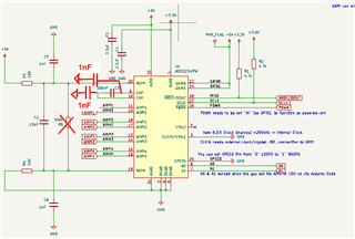
Thus, I need to use your ADS1234 PWG4 28-pin 4 channel chip.
I have never worked with this chip before and could really use your help and advice on how to set it up. I wish to put it on a PCB along with an Arduino NANO and a CANBUS moduel (MCP2515), and read the incoming strain guage data off of your chip into the Arduino NANO, and then send that data to the MCP2515 canbus module out to the user.
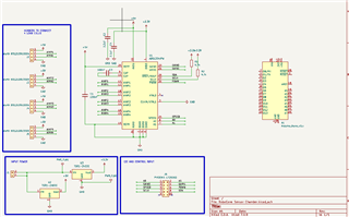
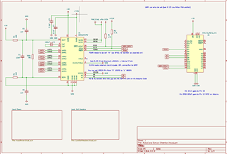
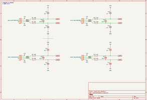
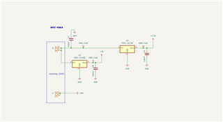
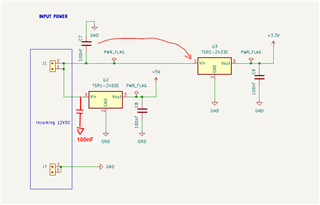
Here is a snapshot of my design with your chip so far. But, I'm not sure if this is right?
Also, do you have any sample code for an arduino to capture the 4 channels off the chip? From what I understand, it's a custom communication protocol "SPI-like", which uses "bit-banging"?
Any support and samples you could send me would be great.
Thanks,
Hendrik
I have
Hello Hendrik,
I will follow-up with answers and recommendations tomorrow. Thanks!
Regards,
Keith Nicholas
Precision ADC Applications
Hello Hendrik,
First, a few suggestions regarding your schematics.
1. For the regulators, I suggest adding an input capacitor, 100nF, for each of the regulators, U2 and U3.
2. I see that you have SCLK and DOUT labeled as I2C, but based on your comments, I think you realize these are standard CMOS IO and and the protocol is generally compatible with SPI, not I2C.
3. For each of the inputs, I recommend adding input filters. This will help filter external noise and also provide some amount of over-voltage (ESD) protection for each of the ADC inputs. Please refer to 'A Basic Guide to Bridge Measurements' application note for more details.
Typical RC values are 100Ohm and 10nF/1nF.
Regarding the digital interface, you can use a standard SPI port, but since the data rate is very low, most folks will simply bit-bang the interface. It is a very simple protocol to implement, but unfortunately, TI does not have any example code. However, other folks have generated sample code.
Please refer to the below link for example code using ADS1234 and Arduino. I have not tested this code and cannot make any assurances that it will work, but at a minimum, it should provide a good example for you to implement in your system.
https://github.com/ciorceri/ADS1232
Regards,
Keith
Hi Keith,
Thanks so much for your comments and suggestions. I have taken them on-board and made changes and improved greatly the design.
I was hoping you could have a look and verify(validate?) that I'm on the right track? If so, I can then proceed with breadboarding and programming.
Here are my improvements on the design:
Hello Hendrik,
The input filters should help. For the input voltage regulators (LDO), place a 100nF capacitor directly next to each LDO input pin, a capacitor for each LDO. This helps with power supply noise and proper operation of the LDOs.
For the ADC, you can remove the 100kOhm resistor between REFP and REFN. This was shown in the above schematic to detect a broken sensor, but it will also cause a gain error in your system. You can leave this resistor if preferred, but you will need to calibrate the gain error if you leave it in the circuit.
Also, we do not have this information in the datasheet, but for best noise performance, I suggest adding additional 1nF capacitors from each of the CAP pins to system ground, as shown below.
Also, for all of the filter capacitors in the signal path, including the analog inputs, the reference inputs, and the CAP pins, you should use NP0/C0G type capacitors for best performance. The power supply capacitors can be more common X5R/X74, since these are not directly in the signal paths.
Hope this helps!
Regards,
Keith