This thread has been locked.

If you have a related question, please click the "Ask a related question" button in the top right corner. The newly created question will be automatically linked to this question.

ADS131M04: DC measuring issues.

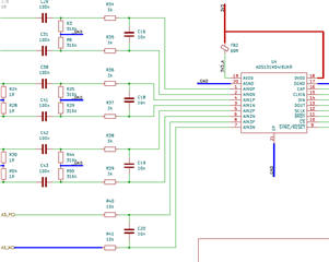
Part Number: ADS131M04
Other Parts Discussed in Thread: TLV3491

Tool/software:

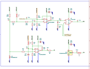
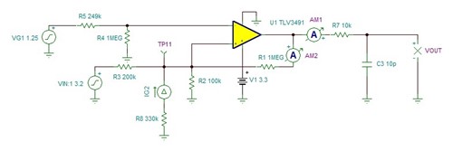
We are measuring the supercap voltage using the 4th channel (AIN3P and AIN3N) of the ADC, as shown in the schematic.
A voltage divider is used to scale down Vsupercap (in this configuration max 3.3V) to a level within the ADC's readable range.

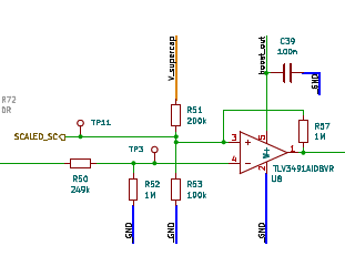
The issue arises when we activate the channel for measurement: we observe a voltage drop at TP11 of approximately 10% compared to the expected level from the divider. However, when the channel is disabled, the voltage returns to the expected value.
According to the datasheet, the ADC's input impedance is 330 kΩ when the gain is set to 1 (our current configuration). Could this be causing the voltage drop when the channel is activated? What would be the best approach to solve this issue?

  • Hi Jonjan,

    Can you please provide the following information so that I can do a simulation for you to check your circuit with different load impedance?

    1. I guess you observed the same voltage drop on the ADC input too and the ADC worked as expected. How much voltage drop did you observe?
    2. Is the 5V or 3.3V used for the power supply to TLV 3491?
    3. The voltage range of Vsupercap?
    4. What's the signal level of SCALED_SC?

    BR,

    Dale

  • Hi Dale,

    yes, the ADC measures correctly.

    1. The voltage drop is almost 10%. For example: The voltage is 1.008V at TP11 when channel is not activated, and it drops to 0.905V when it is activated. The adc measures around 0.9V so I suppose it is measuring correctly.

    2. TLV is powered at 3.3V.

    3. In this configuration is it up to 3.2V because there is an overvoltage protection.

    4. SCALED_SC is defined by the voltage divider created by R51 and R53 so when Vsupercap is 3.2V, SCALED_SC is 1V.

    Best,

  • Hi Jonjan,

    Thank you for your information. I thought SCALED_SC is another signal that is connected to this node.

    I forgot to ask you one more question, where is R50 connecting? It looks like you are using this op-amp (TLV3491) as a buffer between the resistor divider and the ADC, please let me know if there are other purposes.

    BR,

    Dale

  • Hi Dale,

    R50 is connected to a 1.25V shunt regulator (REF1112AIDBZR). We are using the TLV3491 as a comparator to control the charging of the supercap. TLV output will activate the limit mechanism that will stop the charging of the supercap once the Vsupercap reaches 3.2V.

    Best,

  • Hi Jonjan,

    I apologized I did not notice that this is a comparator. It looks like your TLV output is used to control/drive other circuity as you described, but the circuit is not shown in your schematic. 

    With those limited information, the circuit in the attached file was used to simulate the behavior with different load and the bias current from the load(ADC), the bias current can lead to only few millivoltages variation on the ADC input because you are using a large series resistor, but no big voltage drop was observed on the positive input pin of TLV device. You can add your full circuit into the file for further simulation. I think this phenomenon is probably related to your full circuit, you may have to add a buffer to isolate your circuit from the ADC. You can post the question to the amplifier forum to see if the experts of the amplifier/comparator team have any comments or suggestion.

     E2E_sbom335a.TSC

    BR,

    Dale

  • Hi Dale,

    SCALED_SC is directly connected to A3_P pin and AGND is connected to A3_N pin.

    This is the full circuit of how SCALED_SC is controlled and manipulated.

    nEN enables and disables Q2 that controls the charging of the supercap.

    If you require further information regarding the schematic please let me know.

  • Hi Jonjan,

    I modified my comments because I noticed that you mentioned 'SCALED_SC is directly connected to A3_P pin and AGND is connected to A3_N pin'. This information is very helpful for me to understand the phenomenon you mentioned.

    If you put a 330kohm resistor to TP11 position in the simulation file as shown below, the divided voltage at TP11 will be changed from 1.0V to ~1.24V because the 330kohm resistor is close to the value of the resistors in the resistor divider, and also the resistor network will have an additional error that is generated by the input bias current and the large value of resistors you are using. Please notice that I used a typical value of the parameter for the simulation so the changed voltage is a little bit different from what you observed in your circuit. If this is not expected, you need a buffer between SCALED_SC and the ADC input (A3_P).

    I hope this helps you understand, let me know if you have any other questions.

    BR,

    Dale