This thread has been locked.

If you have a related question, please click the "Ask a related question" button in the top right corner. The newly created question will be automatically linked to this question.

DAC80501: ERROR USING dac80502 eval board (DAC80501)

Part Number: DAC80501

Tool/software:

Hello!

I am creating a little software to test the DAC80501 by using the EVAL DAC 80502 board.
I am controlling it by an external stm32 board, since the SOFTWARE provided by TI does not work.

i have attached my set up, where brown cable is CLK, green MOSI, blue CS and white GND.

I am also supplying 5 V (or 3v3 i have tested both) to the board through the bananas cables.

Note:

  • J5 is placed to have SPI communication (PIN 4 to GND)
  • PIn 2 of j11 is connected to the clk 
  • pin 2 of j8 is connected to Mosi
  • The right side of j13 is used to drive CS 

This is my code, very simple:

  uint8_t disableRef[3] = {0x03, 0x01, 0x00};
  
  uint8_t data1[3] = {0x08, 0xFF, 0xFF}; //DAC DATA FULL

  uint8_t data2[3] = {0x08, 0x00, 0x00}; //NO DATA
  
  
// SEE IF I CAN DEACTIVATE THE INTERNAL REFERENCE
  HAL_GPIO_WritePin(SPI_1_CS_GPIO_Port,SPI_1_CS_Pin, GPIO_PIN_RESET);

  HAL_SPI_Transmit(&hspi1, disableRef, sizeof(disableRef), 1000);

  HAL_GPIO_WritePin(SPI_1_CS_GPIO_Port,SPI_1_CS_Pin, GPIO_PIN_SET);


  while (1)
  {
    /* USER CODE END WHILE */

    /* USER CODE BEGIN 3 */
    
    //MAKE A SQUARE WAVE

	  HAL_GPIO_WritePin(SPI_1_CS_GPIO_Port,SPI_1_CS_Pin, GPIO_PIN_RESET);

	  HAL_SPI_Transmit(&hspi1, data1, sizeof(data1), 1000);

	  HAL_GPIO_WritePin(SPI_1_CS_GPIO_Port,SPI_1_CS_Pin, GPIO_PIN_SET);

	  HAL_Delay(1);

	  HAL_GPIO_WritePin(SPI_1_CS_GPIO_Port,SPI_1_CS_Pin, GPIO_PIN_RESET);

	  HAL_SPI_Transmit(&hspi1, data2, sizeof(data2), 1000);

	  HAL_GPIO_WritePin(SPI_1_CS_GPIO_Port,SPI_1_CS_Pin, GPIO_PIN_SET);

	  HAL_Delay(1);

  }

I have tested this code without deactivating the internal reference ( i mean, using 2.5 V from the chip, without providing external reference). However, it did not show anything. 
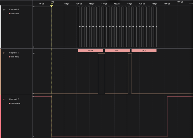
Then, i wanted to test if the device was responding, so I tested if i could deactivate the internal reference by setting 1 to the REF_DIV bite:

  uint8_t disableRef[3] = {0x03, 0x01, 0x00};


However, the voltage reference stills there...

I have attached also some digital captures of the SPI transmission with my oscilloscope and saleae:


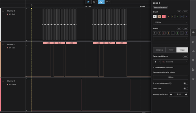
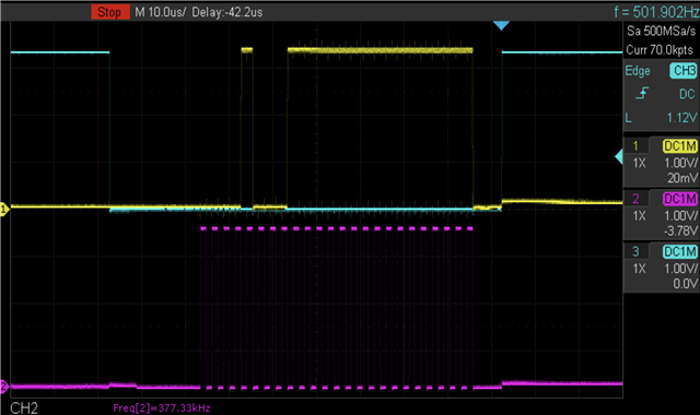
as you can see, everything seems to work fine, however, i do not know why the chip is not responding... May it be broken?

  • Maxim,

    The first thing that I see is that you have the SPI transmission to SDIN set up incorrectly. The data on SDIN is changing at the same time as the falling edge of SCLK and for this device, the SDIN should be changing on the rising edge of SCLK. This means that the SPI mode is wrong. You have the controller set to mode 0, and you should have it set to mode 1 or mode 3, where the data is read on the falling edge of SCLK.

    The following is the timing diagram for the DAC80501. Just make sure the scope matches the diagram.

    Joseph Wu

  • Hi, Joseph.

    Thank you for your quick response.

    I have change the mode of the SPI to 1 (cpol = 0, CPHA = 1):


    and this is what i got through the digital analyser:

    as you can see, it seems i am writing the correct data to the chip registers. However, the 2,5 V still there.

    My code is:

      uint8_t disableRef[3] = {0x03, 0x01, 0x00};
    
      HAL_GPIO_WritePin(SPI_1_CS_GPIO_Port,SPI_1_CS_Pin, GPIO_PIN_RESET);
    
      HAL_SPI_Transmit(&hspi1, disableRef, sizeof(disableRef), 1000);
    
      HAL_GPIO_WritePin(SPI_1_CS_GPIO_Port,SPI_1_CS_Pin, GPIO_PIN_SET);
    

    do you know what may be happen?

    regards,

  • Maxim,


    The one thing I noticed in your plot is that the /CS (/SYNC) and the SCLK occur at the same time in the plot. If the /CS goes down first then that coincident edge may be interpreted as the first SCLK. That would shift the data in the register over by one and change the communication.

    If you can't get the SCLK to idle low before /CS goes low, then you may want to change the SPI mode to 3 (where the clock idles high and the data is transferred on the falling edge). Another thing to test would be to use the EVM with the GUI connected through the USB cable. This should be able to control the EVM correctly. Once you are able to communicate with the EVM and control the functions, you can use the logic analyzer to show the SPI communication. After that, you'll be able to match the communication using the analyzer plots as a template.


    Joseph Wu

  • Hi, Joseph!

    Thank you for your help.

    In the end, I was right, the DAC was broken. I bought one new and it worked. 

    Thank you very much for your help. I will mark the previous answer as "accepted solution" :)