This thread has been locked.

If you have a related question, please click the "Ask a related question" button in the top right corner. The newly created question will be automatically linked to this question.

ADC3424: What does the ADC3424's "6.6kΩ // 3.7pF" differential impedance mean?

Guru 12235 points
Part Number: ADC3424

Tool/software:

Hi,

I am currently evaluating the ADC3424 for a differential signal acquisition circuit.

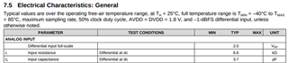
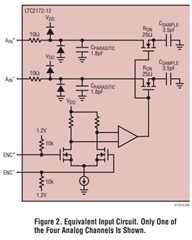
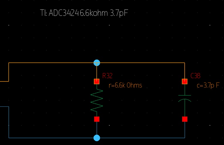
We understand that this is the equivalent impedance seen across VIN+ and VIN−. However, for purposes such as driver design and simulation modeling, we would like to accurately represent this input behavior.

1. A direct differential model: 6.6kΩ resistor and 3.7pF capacitor connected in parallel across VIN+ and VIN−

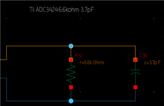
2.A symmetrical model: 3.3kΩ resistor and 1.85pF capacitor connected from each of VIN+ and VIN− to ground (so that the total differential impedance equals 6.6kΩ // 3.7pF)

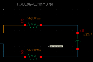
Could you please advise which of the following two circuit models is the correct or recommended way to represent the input characteristics?

Thanks,

Conor

  • Hi Conor,

    Please use the first method. Typically the lumped parallel R||C is given in the datasheet to work with.

    If you need follow on help with the analog input circuitry please let me know. We are happy to help.

    Regards,

    Rob

  • Hi Rob,

    We received an inquiry from a customer currently evaluating ADC3424, and would like to confirm the following points.

    TI’s ADC3424 specifies a differential input impedance of 6.6kΩ // 3.7pF, whereas ADI’s LTC2172-12 appears to have an input structure resulting in approximately 35Ω // 5.3pF.

    While we understand this difference is due to architectural and modeling differences, we would appreciate your confirmation on the following:

    1. Is the 6.6kΩ // 3.7pF model intended to represent the average differential load across the input pins of ADC3424?

    2. Can we assume the difference from ADI’s specification is due to differing internal input structures, and that the values stated in the TI datasheet are accurate?

    Thanks,

    Conor

  • Conor,

    Regarding #1, the 6.6kΩ and 3.7pF are specified for DC. The response of the ADC input is frequency dependent. The datasheet shows the R//C vs frequency in Figure 181 and Figure 182. I cannot talk about the competitor device, however it must be specified at a specific frequency or show a plot as this will always be non-linear.

    Regarding #2, yes, the ADC architecture and packaging directly impacts the parasitics of the ADC. It's normal for this to change across ADC's unless they are within the same device family, and even then it may be slightly different. 

    Thanks, Chase

  • Hi Conor, a good way to model the input parallel R||C is documented here.

    www.electronicdesign.com/.../high-speed-adc-input-impedance-a-measured-versus-a-mathematical-approach

    You can also use this spreadsheet for the customer as well. Please see attached.

    If they have any other questions please let us know.

    I will close this post for now.

    Thanks,

    Rob

    AIN_DIFF_ZIN-ADC3424.xlsx