This thread has been locked.

If you have a related question, please click the "Ask a related question" button in the top right corner. The newly created question will be automatically linked to this question.

ADS131B02-Q1: Switching CHn_CFG from Test Signal to AIN1P/AIN1N

Part Number: ADS131B02-Q1
Other Parts Discussed in Thread: ADS131B04-Q1EVM

Tool/software:

Hi Ti Support Team,

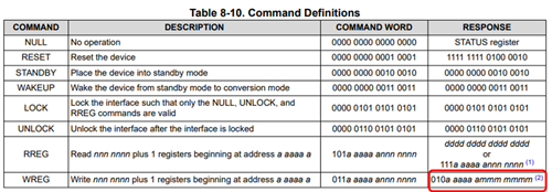
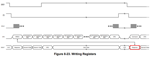
I am currently using the CH1_CFG setting to 10b (Positive DC test signal) to output a test signal and calculate Vref. This is primarily for use in the initial-stage inspection process, to check if the Vref value is within normal limits. However, after outputting the test signal and calculating Vref, when I change the CH1_CFG setting to 00b (AIN1P and AIN1N), the ADS131B02 encounters an issue. Both the WREG and RREG commands are not functioning correctly.

Could you please guide me on the correct procedure to handle this situation? I would appreciate your assistance in resolving this issue.

Thank you for your support.

BR

Stephen

  • Hi Stephen,

    Did your WREG and RREG work without switching the internal MUX? Can you send a logic analyzer plot showing the communication signals from/to the ADC for setting CH1_CFG register, sending WREG and RREG commands with the feedback from the ADC?

    BR,

    Dale

  • Hi Dale,

    Both WREG and RREG operations are functioning correctly.
    Since the ADS131B02 has already been integrated onto the PCB and enclosed within the mechanical housing, I am unable to probe internal signals to verify the waveforms directly.

    My ADS131B02 configuration sequence is as follows

    1. Perform WREG to configure registers 0x03, 0x04, and 0x06(including CLK, OSR, Gain, Chopping mode and GC_DLY confuguration).
    2. Perform RREG to verify that 0x03, 0x04, and 0x06 were correctly set.
    3. Perform WREG again to update registers 0x0E and 0x06 to configure CHn_CFG and disable chopping mode.
    4. Insert a 1 ms delay.
    5. Read ADC values from channel 1, which outputs a test signal, and use it to calculate Vref.
    6. Perform another WREG to update 0x0E and 0x06 to switch CH1_CFG from Positive dc test signal to AIN1P and AIN1N  and enable chopping mode.
    7. Perform RREG to verify the updated values of 0x0E and 0x06.  → However, the values read back differ from the ones written.

    Even if I skip the RREG step, the ADC output code used to calculate current still appears incorrect.
    Therefore, I suspect that the final WREG operation (to enable chopping mode by updating CH1_CFG) may not have executed successfully.

  • Hi Stephen,

    If your WREG worked before writing before the step 6, your WREG should work in the step 6 as well. It will be easy to figure out the root cause by checking your timing.

    I have one question or suggestion for you, did you send one more frame to the ADC after you sent the WREG command in the step 6? If so, you should be able to see the following response for your WREG command from the ADC. The response should shown on the first word in the next frame as you can see the timing below.

    BR,

    Dale

  • Hi Dale,

    I found that there seems to be an issue during the step 5 when reading values, and I’d like to confirm with you.
    If I have CRC enabled and I want to read values from 2 channels at once, is the SPI Command frame:
    {0x00, 0x00, 0x00, 0xCC, 0x9C, 0x00, 0x00, 0x00, 0x00, 0xCC, 0x9C, 0x00}?

    BR,

    Stephen

  • Hi Stephen,

    Your data seems incorrect for reading conversion data, the first word should be the STATUS with the value of 0x05 03 00 ('3' in hex indicates DRDY1 and DRDY0 bits in the STATUS register were set and the data are ready).

    Below is the timing of normal operation that was captured on ADS131B04-Q1EVM (we do not have an EVM board for B02 but the difference between those two ADCs is the channel count):

    In the timing, the frame includes STATUS word + CH0 data + CH1 data + CH2 data + CH4 data + CRC word in 24-bit word length.

    The CRC checksum from the B04 ADC in this timing is 0xC6A9, this is the correct checksum for the data '050F00FFF8DCFFFC65FFFAB1FFF85D', see the screenshot below (this was checked with one of the free online tool: https://www.lammertbies.nl/comm/info/crc-calculation):

    Please note the CRC calculation on the ADS131B0x-Q1 is initialized with the seed value of 0xFFFF.

    BR,

    Dale

  • Hi Dale


    Sorry, let me clarify further.
    I'm referring to the SPI command sent from the host. According to the datasheet, reading the ADC conversion data involves sending a NULL command.

    I’d like to confirm if the RX_CRC_EN feature is enabled, what should the format of this command be?
    Or is it possible that I’ve misunderstood something?

  • Hi Stephen,

    Please check the details for the input CRC in the query below, this  is same for ADS131B0x:CRC difficulties

    CRC difficulties

    BR,

    Dale

  • Hi Dale,

    Got it, I understand.
    Thank you very much for your assistance!

    Stephen

  • Hi Dale,

    I apologize for not paying attention to the status register at that time. I’m currently able to correctly get the values from channel 0 and channel 1, but the CRC_ERR bit in the STATUS register is always set.
    I would also like to confirm the behavior of my DIN and DOUT signals with you.

  • Hi Stephen,

    If you could check the data in this frame according to the method I introduced, you should be able to see all the CRC data in the frame you shared are correct.

    The CRC_ERR bit in the STATUS register in this frame indicates that you had a CRC error in the previous frame, so you have to check your data in the previous frame.

    BR,

    Dale

  • Hi Dale,

    I solved this problem, thank you for your help!

    BR,

    Stephen

  • Hi Stephen,

    Thank you for your update. I'm glad to hear this good news from you.

    BR,

    Dale