This thread has been locked.

If you have a related question, please click the "Ask a related question" button in the top right corner. The newly created question will be automatically linked to this question.

ADS8568: SPI interface to ATMEGA2560

Part Number: ADS8568

Tool/software:

Hi

Has anyone been able to interface via SPI an ATMEGA2560 to an ADS8568?

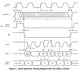
In my current application, the ADS8568 is layout to operate in serial mode.
Until now I have been unsuccessful in getting readings back on the MISO line.

After looking at the spec sheet for ADS8568, it's timing requirements appear to be a lot more demanding than what the ATMEGA2560 can do.
(It looks like it was made to work with C2000 or FPGAs)
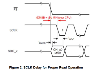
For example this :
Care should be taken to ensure that the delay time of
the most significant bit (tDMSB) from the falling edge of FS/CS is met before applying the serial clock. This
delay is specified as 12 ns MAX

Since ATMEGA works at 16MHZ, its fastest instruction will be in 62nS!

Am I right in thinking the ATMEGA2560 will not be able to communicate via SPI to the ADS8568?

Any help would be appreciated.

  • Hello PowerGuy, 

    Thank you for posting on TI's E2E Forum! 

    The ATMEGA2560 has not specifically been tested, but the ADS8568 uses SPI Protocols CPOL=1, CPHA=0 and has a SCLK speed range from 100kHz to 45MHz, so the 16MHz (or even 8MHz) of the ATMEGA2560 for SPI configuration sounds possible. 

    You are correct though, the ADS8568 can be demanding in its requirements depending on how the device is used. These devices can be quite complex and have vast configuration options that allow microcontrollers like the C2000 as well as FPGAs use the device beyond the standard SPI ADC. 

    Another added benefit of all this configurability is that, it can also be used with more straightforward configurations while still benefitting from its high performance. So C2000 or FPGAs are not always needed. 

    Could you please share the configuration you would like to use the ADS8586?

    If you could please share a schematic as well as an oscilloscope or logic analyzer screen shot of what the current digital communication looks like that would be helpful to understand why read backs have been unsuccessful. 

    To address your tDMSB concern, that quote shared comes from ADS8528, ADS8548, ADS8568 Timing Considerations, which is an application note that focuses on the timing requirements to achieve the full-speed of those devices, using an external clock, and is indeed made with a focus on the C2000+ controllers. In order to enable the maximum data throughput, care should be taken to configure the communication to use the minimum timing requirements, but there are other methods to use this device too.

    Even then, this is a specification of a digital output pin of the device, so a maximum value is used to express the high performance of the device, and not necessarily the requirement of the controller. In that same User's Guide, it expresses that tDMSB is used to determine the delay between FS and SCLK for proper read operations using the equation tDMSB + tSU min. tSU min is not explicitly stated in the datatsheet, but it is correlated to the speed of the SCLK, which for this device should be between 100kHz to 45MHz, allowing plenty of margin. 

    tDMSB is the delay from when FS (Frame Synchronization) goes low to when the MSB data is valid on SDO. The maximum value is 12ns, which means that after the FS goes low the MSB data will take no more than 12ns to transition to the valid MSB bit value. This value will remain in that state until the falling edge of the serial clock (SCLK), after that it will remain at that value for at least 5ns (tHDO), but no more than 17ns, because 17ns (tPDDO) or less after the SCLK falling edge the next data bit will be set on SDO, and so on until the 16 bit frame is complete (or 32 depending on how it is configured). Making the SDO output dependent on the SCLK input. 

    Meaning that when using serial mode the delay between FS going low and SCLK going low should be between: 

    • Highest speed on SCLK (45MHz) : tDMS + (tSCLKmin - tPDDO) = 12ns + (22ns - 17ns) = 17ns
    • Slowest speed on SCLK (100kHz): tDMS + (tSCLKmax - tPDDO) = 12ns + (10us - 17ns) = ~10us

    tSCLK - tPDDO was used instead of tSU,

    Also, please note that using the internal conversion clock (CONFIG bit C29 = 0)  instead of an external conversion clock (XCLK input pin & CONFIG bit C29 = 1), allows for a simpler and slower approach when communicating to the device as well. 

    Best regards, 

    Yolanda

  • Good morning,

    thank you for your response. 
    The ATMEGA2560 is able to communicate with the ADS8568.
    I was not configuring the ADC properly. (the RESET pin was high)


  • Good morning!

    Glad to hear the ATMEGA2560 was able to communicate! Thank you for letting me know!

    Best regards, 

    Yolanda