This thread has been locked.

If you have a related question, please click the "Ask a related question" button in the top right corner. The newly created question will be automatically linked to this question.

TLA2518: TLA2518 SPI Readback: Random / Glitchy Data When Reading Unconnected or Non-AVDD Inputs

Part Number: TLA2518

Tool/software:

Hi TI team,

I'm currently bringing up the TLA2518 with a Cyclone V E FPGA via SPI. I’m operating in SPI Mode 0 (CPOL = 0, CPHA = 0), using On-the-Fly mode, and following the recommended frame format.
My SPI Setup:

  • Clock frequency: 31.25 MHz (generated from 125 MHz system clock ÷ 4)

  • SPI Mode: Mode 0 (clock idles low, data sampled on rising edge, data driven on falling edge)

  • Command frames: Always 24 bits long during CS low (e.g., 0x08 0x10 0x02 to set SEQ_MODE)

  • Readback: Occurs in the next SPI frame, CS held HIGH between frames for >3.6 μs (450 system clocks) to allow conversion

  • MOSI (SDO): Driven on falling edge of SCK

  • MISO (SDI): Sampled on rising edge of SCK

  • After initialization, I’m sending the 12-bit on-the-fly channel select frame: 12'b 100100000000 (to select channel 2)

Behavior:

  • When I connect AVDD to AIN2, I get expected results (e.g., 0xFFF).

  • When I connect other voltages (e.g., 1.2 V, 2.0 V) or leave AIN2 floating, I receive random values such as: 0x820, 0xC08, 0x408, 0x402, 0x000

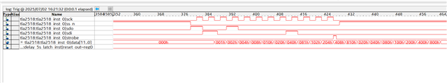
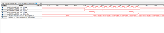
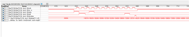
  • SignalTap waveform shows:
    • sdo transitions correctly on falling edge
    • sdi is not stable for a full SCK period — it appears to change mid-bit
    • MISO values look corrupted even though CS, clock, and timing all match datasheet spec

Questions:

  • Should each SDI bit remain valid for one full SCK cycle at 31.25 MHz?

  • Is SPI Mode 0 supported for continuous readout, or is Mode 1 required for stable SDI timing?
  • Could unstable sdi be due to ADC output tri-stating or signal integrity?
  • Do you recommend adding a pull-up/down or series resistor on SDI?


I’ve attached:
SignalTap waveform screenshots
Connection schematic

  • Hi TI team,
    Any update on this? I am attaching my verilog code and sdc file details.

  • Hi Sameer,

    Sorry to get to this late. I was out of office for the majority of the past week. 

    You shouldn't have any issues running the interface at a full 60MHz, in SPI Mode 0. I am able to operate at maximum speeds with no issue from the device without an issue.

    The confusing part on my end was that SDI and SDO on your logic captures is labelled in reference to the controller, so from the device, they are flipped. It would be useful to have one labelled as MOSI and MISO.

    I'm not sure why the device's SDO would not stay high the entire SCLK cycle. That is not something I have observed before. If you probe the lines with an oscilloscope, do you see the same behavior?

    There could be signal integrity issues. I would first start by testing the same sequence at slower clock frequencies. Another thing to consider is how long ~CS is held high between conversions. What is this period? At a minimum it should be 600ns.

    Regards,
    Joel

  • Hi Joel,
    Thanks for your response. Now I am getting stable value after I added a pull down registor in between MISO pin and SDO pin of TLA2518 at a frequency of 15.75MHz. But i am getting almost half value when I am operating it at 31.5MHz. My CS duration is high for exactly for 600ns. Shall i increase CS high duration (in my design CS is high for 600ns & CS is low for 400ns) for one time capturing the data in on fly mode. Any suggestion on this? Why i am not getting the desired result? I am attaching my verilog code and sdc files below for your references.

    // tla2518.v -- (c)2025 Coherent Corp.
    
    
    /* 
    
    //SPI interface for TLA2518 ADC using On-the-Fly mode
    	 Assumes 125 MHz system clock (8 ns period)
    	 SCK = 31.25 MHz (1 SPI bit = 4 clk cycles = 32 ns)
    
    // PHASE 1: Mode set (SEQ_MODE = 10b)
    	 - SPI write of 24 bits: 0x08 0x10 0x02
    	 - CS held LOW for 98 clk = ~784 ns
    	 - Sets ADC to On-the-Fly mode
    
    // PHASE 2: Channel select + acquisition
    	 - SPI frame with first 5 bits: 2’b10 + 3-bit CH ID
    	 - CS held LOW for 50 clk = ~400 ns = tACQ
    
    // PHASE 3: Conversion
    	 - CS goes HIGH → ADC begins SAR conversion
    	 - Wait 75 clk = 600 ns (> tCONV = 600 ns)
    
    // PHASE 4: Data read
    	 - Next SPI frame (during CS LOW), shift in 12-bit ADC result
    	 - Shift 1 bit every 4 clk (SCK = 31.25 MHz), strobe asserted at bit 48
    	 - `data[11:0]` = ADC value, `addr` = channel
    
    */


    module tla2518(
    	input clk,						// 125 MHz system clock
    	input reset,					// Active-high reset
    	input sdi,						// Serial data input (SDO from ADC)
    	output reg sck,					// SPI clock to ADC (31.25 MHz)
    	output reg sdo,					// SPI data out to ADC
    	output reg ss_n,				// SPI chip select (active low)
    	output reg [2:0] addr,			// Channel address for tracking
    	output reg [11:0] data,			// 12-bit ADC output
    	output reg strobe				// High when new data is valid
    );
    
    
    	// assume 125MHz clock (8ns period)
    	// Register write (CS low) 784ns = 24 * 32ns + 16ns = 98 * 8ns
    	// Acquisition (CS low) 400ns = 12 * 32ns + 16ns = 50 * 8ns
    	// Conversion (CS high) 3.6us = 450 * 8ns
    	
    	
    	localparam
    		s_init = 2'd0,					// Phase 1: Initialization
    		s_run0 = 2'd1,					// Phase 2: Channel select
    		s_run1 = 2'd2;					// Phase 4: Data read
    
    	parameter chan = 3'd2;				//Read data from only channel 2
    	
    	
    	reg [8:0] active;					// Controls how long CS stays LOW
    	reg [0:31] command;					// SPI command (32-bit container, top 24 bits used)
    	reg [7:0] frm_duration;			//It will explain how much duration fram will run
    	
    	//reg [2:0] chan;				// Channel number to select
    	reg [8:0] count;			// Global cycle counter (0 to 499)
    	reg [1:0] state;			// FSM state register
    	
    	always @(*) case(state)
    		s_init:
    			begin
    				active = 9'd98;						// CS active for 24.5 SCK periods // Phase 1: 24-bit write → 24 bits × 4 clk = 96 clk + 2 clk slack = 784 ns
    				command = 32'h08_10_02_00;			// Write SEQ_MODE = 0x02 (On-the-Fly mode); 
    				frm_duration = 8'd173;				//98 clk cs low + 75 clk cs high (600ns conversion time)
    			end
    		s_run0, s_run1:
    			begin
    				active = 9'd50; // CS active for 12.5 SCK periods
    				command = {2'b10, chan, 27'b0}; // select channel on-the-fly
    				frm_duration = 8'd125;				//50ckl cs low + 75 clk cs high
    			end
    	endcase
    	
    	always @(posedge clk or posedge reset)
    		if(reset) begin
    			//chan <= 3'b0;
    			count <= 9'b0;
    			sck <= 1'b0;
    			sdo <= 1'b0;
    			ss_n <= 1'b1;
    			state <= s_init;
    			strobe <= 1'b0;
    		end else begin
    			//if(count < 9'd499)
    			if(count < frm_duration)
    				count <= count + 9'b1;
    			else begin
    				count <= 9'b0;
    				case(state)
    					s_init:
    						state <= s_run0;
    					s_run0, s_run1:
    						begin
    							addr <= chan;
    							//chan <= chan + 3'b1;
    							state <= s_run1;
    						end
    				endcase
    			end
    			if(count[1:0] == 2'b0)
    				data <= {data[10:0], sdi};							// Serial data input (SDO from ADC) from every 4th clock cycle +ve edge of sck
    			strobe <= (state == s_run1) & (count == 9'd48);
    			sck <= (count < active) & count[1];					//its performing frequency divide by 4
    			//~|count[8:7] prevents to send beyond 24 bit i.e., 24*4 = 96 clk clk after that sdo will be 0
    			sdo <= ~|count[8:7] & command[count[6:2]];			//command[count[6:2]] picks one bit from the 32-bit command word
    			ss_n <= ~(count < active);							// CS LOW during active phase
    		end


    endmodule
    

    # Base input clock: 24 MHz
    create_clock -name clock_osc -period 41.667 [get_ports clock_osc]
    derive_pll_clocks
    derive_clock_uncertainty
    
    #set clk pll1_0002_inst|altera_pll_i|general[0].gpll~PLL_OUTPUT_COUNTER|divclk
    #give some name to pll generated output and we are giving clk_125M
    set clk_125M pll_1|pll1_0002_inst|altera_pll_i|general[0].gpll~PLL_OUTPUT_COUNTER|divclk
    
    #set clk_62_5M pll_3|pll3_0002_inst|altera_pll_i|general[0].gpll~PLL_OUTPUT_COUNTER|divclk
    
    #we are defining the clock for the particular registor
    create_generated_clock -name sck_reg -source [get_pins $clk_125M] -divide_by 4 tla2518_inst_0|sck
    
    #create_generated_clock -name sck_reg -source [get_pins $clk_62_5M] -divide_by 4 tla2518_inst_0|sck
    
    #Now we have to define the clock for particular pin
    create_generated_clock -name sck -source tla2518_inst_0|sck [get_ports sck_o]
    
    
    #wrong parameters defines so that future someone will understand it
    #create_generated_clock -name sck -source [get_ports $clk] -divide_by 4 [get_ports {Top_TLA2518|tla2518_inst_0|sck}]
    
    
    #we have to define the input and output delay based on datasheet of tla2518
    set_input_delay -clock sck -clock_fall -max 16.0 [get_ports sdi]
    #set_input_delay -clock sck -clock_fall -min 0.0 [get_ports sdi]
    
    set_multicycle_path -from sdi -setup -end 4
    set_multicycle_path -from sdi -hold -end 3
    
    
    set_output_delay -clock sck -max 1.5 [get_ports sdo]
    set_output_delay -clock sck -min -2.0 [get_ports sdo]
    
    set_multicycle_path -to sdo -setup -start 2
    set_multicycle_path -to sdo -hold -start 3


  • Hi Joel,
    I have one more questions. Do we need any other timing parameters needs to be added in SDC file. Because according to my understanding if my code is working for low frequency, but not for high frequency then there must be some timing issue. I didn't set tDEN_CSDO & tDZ_CSDO time i.e., with respect to cs pin. Can you please suggest, how to set these timings by looking at my code. Then it will be helpful to me.

  • HI Sameer,

    For debugging signal integrity issues, I think it would be useful if you shared a schematic and oscilloscope captures of the SPI lines. It could be that the SCLK line is too noisy. The Verilog is helpful, but it is more beneficial to see the actual results that it produces in the analog realm.

    At the moment, how are you prototyping your design? Do you have a PCB built, or are you using a breadboard? Do you have a logic analyzer available (a Saleae for example) that might help inspect the timing parameters a little bit closer?

    Regards,
    Joel

  • Hi Joel,
    I am using  a breadboard setup first to bring the ADC once it is done then we will integrate in our PCB design. We don't have any external logic analyzer apart from Quartous Prime (Signal Tap Logic Analyzer). Can I take 13 bit data and discard LSB or once CS is low, we set MOSI (of my FPGA) set to low and after that I will send data of 12 bit (means 13 bits of transaction).

  • Hi Sameer,

    Thanks for the info. This current implementation seems likely to be causing issues, especially at high clock frequencies. Once it is all integrated on a PCB, I would expect these issues to go away, as SPI is actually not especially demanding in terms of maintaining signal integrity.

    Are you able to send oscilloscope captures instead then, making sure that the ground probe is as short as possible to reduce external noise pickup, and at least for SCLK, using ground spring probe? The SDO behavior from the device does not seem normal, so I'm wondering if there are some false SCLK edges being picked up.

    You should be able to send 13 SCLKs and still get data as expected. I think you are viewing it from the perspective of what is sent from the FPGA, but from the device perspective, it will send ADC conversion data on SDI as long as a register read command hasn't been sent in the previous frame.

    Is the sampling rate on the logic analyzer configurable? If so, what speed are the digital signals sampled at?

    Regards,
    Joel

  • Hi Joel,
    Shall I send my complete archive file and you can extract it and test it and suggest me whether is it a setup error from my side or something else. Its very important for me and its high priority for me. I am attaching my archive file. You can use it by using quartous prime tool. Please try it from your end. I used oscilloscope, but waveform are quite noisy. If you seggest something then it will be hepful to me. Can we have a call regarding this?

  • module Top_TLA2518(
    	input clock_osc,
    	input sdi,						// Serial data input (SDO from ADC)
    	output sck_o,					// SPI clock to ADC (31.25 MHz)
    	output sdo,					// SPI data out to ADC
    	output ss_n,				// SPI chip select (active low)
    	output strobe
    	//output clk
    );


    	wire clk;							//125MHz
    	wire clk_62_5m;
    	wire clk_250m;


    	wire sck_i;
    	wire [1:0] pll_locked;
    	//assign sck_o = sck_i;
    	
    	
    	wire pll_locked_w = &pll_locked;
    	reg [1:0] pll_ready;
    	assign reset = ~pll_ready[1];
    	assign po_reset_int = ~pll_ready[1];
    	wire [11:0]data;
    	
    	
    	tla2518 tla2518_inst_0(
    		.clk(clk),
    		//.clk2(clk_250m),
    		.reset(reset),
    		.sdi(sdi),
    		.sck(sck_o),
    		.sdo(sdo),
    		.ss_n(ss_n),
    		.addr(),
    		.data(data),
    		.strobe(strobe)
    	);


    	always @(posedge clk or negedge pll_locked_w)
    		if(~pll_locked_w)
    			pll_ready <= 2'b0;
    		else
    			pll_ready <= {pll_ready[0], 1'b1};
    			
    	pll1_0002 pll_1(
            .refclk    (clock_osc),   //  refclk.clk
            .rst       (1'b0),      //   reset.reset
            .outclk_0  (clk), // outclk0.clk 125MHz
            .locked    (pll_locked[0])//  locked.export
        );
    	 
    	 
    	 pll2_0002 pll_2(
            .refclk    (clock_osc),   	//  refclk.clk
            .rst       (1'b0),      		//   reset.reset
            .outclk_0  (clk_62_5m), 			//sampling clock for debugging 250MHz 
    		  .outclk_1  (clk_250m),
            .locked    (pll_locked[1])	//  locked.export
        );


    endmodule

  • This is my top level verilog code

    create_clock -name clock_osc -period 41.667 [get_ports clock_osc]
    derive_pll_clocks
    derive_clock_uncertainty
    
    
    set clk_125M pll_1|pll1_0002_inst|altera_pll_i|general[0].gpll~PLL_OUTPUT_COUNTER|divclk
    
    set clk_62_5M pll_2|pll2_0002_inst|altera_pll_i|general[0].gpll~PLL_OUTPUT_COUNTER|divclk
    
    create_generated_clock -name sck_reg -source [get_pins $clk_125M] -divide_by 4 {tla2518_inst_0|sck tla2518_inst_0|ss_n}
    create_generated_clock -name sck -source tla2518_inst_0|sck [get_ports sck_o]
    
    create_generated_clock -name adc_ss_n -source tla2518_inst_0|ss_n [get_ports ss_n]
    
    #we have to define the input and output delay based on datasheet of tla2518
    set_input_delay -clock sck -clock_fall -max 16.0 [get_ports sdi]
    set_input_delay -clock sck -clock_fall -min 0.0 [get_ports sdi]
    set_input_delay -clock adc_ss_n -clock_fall -max 15.0 [get_ports sdi] -add_delay
    set_input_delay -clock adc_ss_n -clock_fall -min 0.0 [get_ports sdi] -add_delay
    
    set_multicycle_path -from sdi -setup -end 4
    set_multicycle_path -from sdi -hold -end 3


    set_output_delay -clock sck -max 1.5 [get_ports sdo]
    set_output_delay -clock sck -min -2.0 [get_ports sdo]
    
    set_multicycle_path -to sdo -setup -start 2
    set_multicycle_path -to sdo -hold -start 3

  • Dear Joel,

    I hope this message finds you well.

    I have attached the top-level module, the TLA2518 Verilog module, and the corresponding SDC file for your reference. You may compile this code using any standard EDA tool to generate a bitstream file, which can then be tested with the TLA2518 ADC.

    We would greatly appreciate it if you could review the design and suggest any necessary changes or improvements. This ADC interface is a critical component of our ongoing development, and ensuring its proper operation is essential for our system's success.

    If the current implementation functions as expected, we plan to integrate it into our main device and proceed with a bulk order of TLA2518 ADCs through your distribution channels.

    Thank you for your support and assistance. We look forward to your valuable feedback.

  • Dear TI team,

    Any update on my issue?

  • Hi Sameer,

    I typed my response and hadn't sent it. Apologies for that.

    Thanks for sharing the files, and I understand this is high priority. I have sent you a request to connect over private message so that we can correspond over email and set up a call to discuss this issue.

    At the moment, I don't have access to Quartus or Vivado as we have to allocate licenses. Still I think the best way is to take oscilloscope captures in order to observe the behavior of the device, especially as it drives the SDO pin. Please let me know if that is possible. So far, the commands being sent look correct, so I believe this is likely a signal integrity issue, especially since it seems to operate correctly at lower clock frequencies, but shows trouble at higher data rates.

    Regards,
    Joel


  • Hi  ,
    I am attaching my oscilloscope results, below. Please fine the attachment. Please try to compile my verilog code any EDA tool and try to test with your set up, if possible. Then it will be helpful to me. I didn't receive any mail to connect with you in. Can you please specify which platform you send me the link.

  • Hi Sameer,

    Yes, the SPI lines look very noisy. Might you try probing with ground spring probe attached and seeing if you get better results?

    I sent it via E2E. You should see it by checking your notifications or under the friends tab. We can connect privately afterwards.

    Regards,
    Joel


  • Hi  ,
    I didn't receive any notification from you regarding private chart. I connect one end of probe to ground and another one to pins. But still I am getting the same. Do you have any other Idea how to create a clean setup.

  • Hi Sameer,

    I will follow up via private message so we can talk further.

    Regards,
    Joel

  • Sameer,

    I responded over private message a couple of days ago. Please continue this conversation over private message.

    Regards,
    Joel