This thread has been locked.

If you have a related question, please click the "Ask a related question" button in the top right corner. The newly created question will be automatically linked to this question.

ADS8588SEVM-PDK: How do I use use this?

Part Number: ADS8588SEVM-PDK
Other Parts Discussed in Thread: DAC8775EVM, ADS8588S, ADS8584S

Tool/software:

Hello, 


I am using the ADS8588SEVM with my MCU via SPI. I have tried playing around with the EVM using the PHI and can acquire the sine wave I wish to see on the GUI. What I am confused by is when using an oscilloscope to capture the signals I need to recreate with my MCU, I get the attached image. 

  A

Yellow: SCLK
Blue: CONVSTA
Purple: DOUTA

I am trying to capture an analog sine wave with range 0-10V via the DAC8775EVM. I can confirm that the DAC produces the wave and is fully functioning. For the ADS settings, I have set:
Range: -10V to 10V
Serial Interface (with J3 shunted)
Oversampling x0
Internal Reference.

I also have an external AVDD = DVDD = 5V.

Questions.
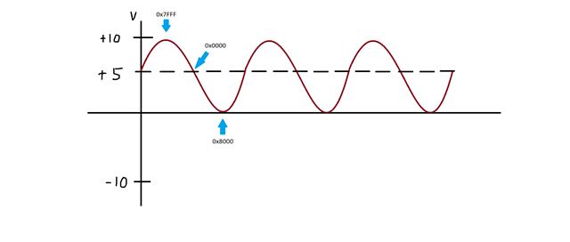
1) How do I understand what is shown in the oscilloscope? I know that there is something about a 2's-complement but I do not fully understand it even after I know I need to convert the DATA into unsigned.

2) What exactly do I need to toggle to successfully replicate the capture in the GUI? From my understanding, I need to toggle CONVSTA, set /CS to low, receive the input, set /CS to high and repeat for continuous capture?

I am quite new to using this device and would appreciate any help. Thanks in advance.

  • Hi Muhammad,

    The scope shows the 4 conversion results from CHAx, the EVM uses both SDOA and SDOB.  In your case if you want all eight channels from SDOA, you would need to send an addition 4*16 = 64 SCLKs to the ADS8588S device.  What your scope did not capture is the BUSY output signal.  You need to pulse CONVST, wait for BUSY to go low, and then apply /CS and your SCLKs to retrieve the conversion results.

  • Hi Tom, thanks for the swift reply. The BUSY signal was not captured in the oscilloscope, so I will see if I have done it correctly when I get back to the lab in a few hours. I am only trying to collect the data from one channel for now, so I have connected JP1-2 (AIN1+) to the DAC while the other 3 inputs are connected to GND. I have left CONVSTB and SDOB unconnected and floating as I am only planning to use the first 4 channels.

    From what I understand from the timing diagrams, first I pulse CONVSTA, set BUSY to high, set /CS to low, send the analog input data, set /CS to high, set BUSY to low? I then repeat this process in a while loop for continuous capture. This is the process that I have in place following Figure 2 and Figure 5 of the ADS8584S datasheet (the ADC that I am using the ADS8588SEVM for). Please advise. Thanks in advance.

  • BUSY is an internal signal, it is an output from the ADS8588S.  The basic idea is that you would use that output from the ADC as an interrupt to your processor.  Maybe you have CONVST tied to a timer for example and every time you pulse it BUSY goes high.  When the conversion sequence is complete, BUSY goes low signaling you to set /CS low and start your SCLKs to get the conversion results out of the device.

  • Hi Tom, I tried measuring BUSY on the oscilloscope this time and this is the waveform I arrived at.


    As you can see, BUSY (blue) is at low when I pulse CONVSTA (yellow) and when /CS is pulsed afterwards (purple). Currently, my code is written as attached below:


    	    // Output sine waves from DAC CH A and CH C
    	    sine_wave_output_dual();
    	    HAL_Delay(5); 
    
    	    // Trigger ADC conversion via CONVSTA pulse
    	    HAL_GPIO_WritePin(ADS_CONVSTA_GPIO_Port, ADS_CONVSTA_Pin, GPIO_PIN_RESET);
    	    HAL_GPIO_WritePin(ADS_CONVSTA_GPIO_Port, ADS_CONVSTA_Pin, GPIO_PIN_SET);
    
    	    // Wait for BUSY to go LOW (ADC conversion complete)
    	    while (HAL_GPIO_ReadPin(ADS_BUSY_GPIO_Port, ADS_BUSY_Pin) == GPIO_PIN_SET) {
    	    printf("BUSY IS UP \n");
    	    }
    
    	    // Activate CS to read data
    	    HAL_GPIO_WritePin(ADS_CS_GPIO_Port, ADS_CS_Pin, GPIO_PIN_RESET);
    
    	    uint8_t rx_buf[2] = {0};
    	    uint8_t tx_buf[2] = {0x00, 0x00};
    	    HAL_SPI_TransmitReceive(&hspi2, tx_buf, rx_buf, 2, HAL_MAX_DELAY);
    
    	    HAL_GPIO_WritePin(ADS_CS_GPIO_Port, ADS_CS_Pin, GPIO_PIN_SET);

    I can't seem to read a BUSY waveform no matter what I tried. This suggests that the conversion has not started/ the ADS is not converting? Please advise. Thanks in advance.

  • If you are still wired into our EVM, have you verified that the STBY pin is logic 1 and the reset pin is logic 0?  You also need to set the parallel data pins to ground when using the serial interface.

  • Hi Tom, I have confirmed that STBY pin is logic 1, however I am not sure where to check reset pin is logic 0 on the EVM as well as where the parallel data pins on the EVM are. You've mentioned something similar in another forum post but I don't see what you're referring to in the datasheet/ user guide. I can only guess it has something to do in J9, but otherwise I can't really see what the next step is. 

  • DBx pin ststus is in the datasheet.  When operating in serial mode, most of the parallel data outputs need to be grounded or held at logic '0'.

  • Hi Tom, I have managed to get the BUSY pulse on my oscilloscope. It turns out I need to pulse the CONVSTB as well in order for the ADS to toggle BUSY. When using the EVM without the PHI, what do you recommend I do to ground those pins, or must I use the PHI to force them to ground?

    Also, when using SPI to receive data from AIN1, the BUSY signal pulses faster than the I can toggle /CS.


    I am currently using a picoscope an unfortunately, have only 2 channels to measure the waveforms. As shown in the image,, BUSY (blue) toggles before the /CS (red) toggles. I currently have it coded like so:

      while (1)
      {
    	    // Output sine waves from DAC CH A and CH C
    	    sine_wave_output_dual();
    	    HAL_Delay(5);  // ~200 Hz loop
    
    	    // Trigger ADC conversion via CONVSTA pulse
    
    
    	    HAL_GPIO_WritePin(ADS_CONVSTA_GPIO_Port, ADS_CONVSTA_Pin, GPIO_PIN_RESET);
    	    HAL_GPIO_WritePin(ADS_CONVSTA_GPIO_Port, ADS_CONVSTA_Pin, GPIO_PIN_SET);
    	    HAL_GPIO_WritePin(ADS_CONVSTB_GPIO_Port, ADS_CONVSTB_Pin, GPIO_PIN_RESET);
    	    HAL_GPIO_WritePin(ADS_CONVSTB_GPIO_Port, ADS_CONVSTB_Pin, GPIO_PIN_SET);
    
    
    	    while (HAL_GPIO_ReadPin(ADS_BUSY_GPIO_Port, ADS_BUSY_Pin) == GPIO_PIN_SET) {
    	    printf("BUSY IS UP \n");
    
    	    // Activate CS to read data
    	    ADS_CS_EN();
    
    	    uint8_t rx_buf[2] = {0};
    	    HAL_SPI_Receive(&hspi2, rx_buf, 2, HAL_MAX_DELAY);
    
    	    ADS_CS_DIS();
    
    
    	    }
    
    	    HAL_Delay(1);


    If I put the /CS toggle line "ADS_CS_EN();" outside of the while loop, it will pulse after busy has gone back to logic 0.

  • Good to see that you have BUSY working now!  There are series resistors on the DBx lines, you could short those to ground.

  • Ah, I see. Based on the datasheet, can I confirm that I short all the DBx pins except DB7 (DOUTA) and DB8 (DOUTB)?

  • Be aware of the dual use pins too, but otherwise yes.

  • Thanks Tom. I am trying to short the resistors by soldering them to GND but accidentally ripped off the copper line connecting RS15 to pin 33 (DB15). How bad is this?

    *EDIT*: I have managed to short the necessary DBx pins to GND (I shorted DB15 directly from U1) and still no DOUTA waveform. I think there should be no major damage to the board other than the fact that I can no longer use the PHI moving forward. Please advise. Thanks in advance.

  • Hi Muhammad,

    There should not be an issue with the ripped off pad.  Are you applying /CS and SCLK after BUSY returns low?

  • Hi Tom, 
    Yes I have applied /CS after BUSY returns low. The tSU_BSYCS is ~12ms which is fine, since the datasheet does not say a maximum time. I managed to acquire a waveform for DOUTA, and I think it looks good but I don't know how to interpret it. Could you provide some clarity for me? 

    Blue: BUSY
    Red: DOUTA

    However, after a while, I do not get this waveform above, and instead get a flatline on DOUTA (logic 0). Instead, I get this:

    Blue: /CS
    Red: DOUTB

    I have channels 2-8 connected to GND and only channel 1 connected to the DAC output. What's going on here? 

    *EDIT: I managed to get the SCLK using SPI going, but it looks funny. I am sending a HAL_SPI_Receive(); SPI message to the ADS which requests for 2 bytes of data since I only care about the data from channel 1. Is this correct or am I supposed to send clock cycles for all 8 channels?


    Blue: SCLK
    Red: DOUTA

  • Hi Muhammad,

    In general, you should be seeing something like you showed with the original post screen shot.  You can't really interpret the SDO without including the SCLK details.

  • Hi Tom, I realised that I set the time division too high, so here's the actual waveform received.


    Blue: SCLK
    Red: DOUTA

    DOUTA toggles between 0xFEFE and 0xFFFF. I understand it to be in 2's complement, but how do I interpret this? For reference, the data it is capturing is supposed to be an analog sine wave that ranges from 0V to 10V, starting from 5V.

    *EDIT": I remembered something mentioned on another forum post about the RESET button S1 before conversion starts and I managed to get the ranging values that I had desired.


    As you can see in the data column the hex values from the ADS input, is varying in increasing and decreasing order which matches my sinewave. What I would like to clarify is: I am currently using the ADS8588SEVM in -10V to +10V range, but my DAC outputs only 0V to 10V. Is the data gathered going to be affected? My sine wave starts at +5V, goes to +10V, back to +5V and then to 0V and back to +5V. When the DAC outputs from 5V to 7V, the hex values captured goes from 0x7FFF to 0xFFFF then back to 0xEXXX at 8V then when it outputs 8V to 10V it goes to 0xCXXX all the way to 0xFFFF. When going from 10V to 0V, it decreases gradually as expected until it reaches 0x0000 and back to 0x7FFF at 5V. The data then repeats when going from 5V to 7V and so on.

  • Hi Muhammad,

    From the standpoint of the ADC code output, 0x7FFF is full-scale positive.  Full-scale negative would be 0x8000 and the mid-scale code would be 0xFFFF or 0x0000.  How are the grounds connected between your DAC and the ADC?

  • Hi Tom,

    The DAC and the ADC's GND is connected to a common point, which is my MCU board's GND pin. Additionally, the external power supply's GND is also connected to the same common point. For the Analog Inputs, Channels 2-8 are connected to the common point GND, with only Channel 1 being connected to the DAC's output. 

    As for the ADC output, does that mean that anything above 0x8000 is negative (in this scenario is above 5V) and anything below 0x7FFF is positive (below 5V)? I would assume that it would be the other way around.

    This is what I assume to be the expected values acquired:


    Instead, at 0V the ADC captures 0x0000. 

  • Take a look at Figure 66 and Table 2.  If you are in the +/-10V range, your 0-10V DAC should give you 0x0000 to 0x7FFF.  One code below 0V is 0xFFFF and at -10V you would have 0x8000.

  • Hi Tom,

    I understand that, but that's not what is captured on my Picoscope. Could the fact that my AIN2-AIN8 being grounded have anything to do with the discrepancy in the expected values vs actual values? 

  • Hi Muhammad,

    No, that should not matter.  From your picture though, at 0V that code should be 0x0000 (not 0x8000) and the dashed line at 5V, that code should be ~0x3FFF (not 0x0000).

  • Hi Tom,

    Thanks for the clarification, I'll review my code to see if I can capture the expected values and get back to you.

  • Hi Tom,

    After testing it for a while and gathering the values, this is what I ended up with:


    Y-axis: Voltage (V)
    X-axis: Sample number


    Here are the first 20 values that I captured (out of 300):

    DAC_Hex DAC_Voltage (V) ADC_Hex ADC_Voltage (V)
    8323 5.123 7FFF 10
    8647 5.245 877F -9.414
    896A 5.368 8FFF -8.75
    8C8B 5.49 949F -8.389
    8FAA 5.612 98CF -8.062
    92C7 5.734 9F7F -7.539
    95E1 5.855 AB7F -6.602
    98F8 5.975 BFFF -5
    9C0A 6.095 B2BF -6.035
    9F19 6.215 BF1F -5.069
    A223 6.334 BFFF -5
    A527 6.451 C7FF -4.375
    A826 6.568 D7FF -3.125
    AB1E 6.684 DFFF -2.5
    AE10 6.799 FFFF 0
    B0FB 6.913 FDBF -0.176
    B3DE 7.026 E23F -2.325
    B6B9 7.138 EF7F -1.289
    B98C 7.248 F9FF -0.469
    BC55 7.357 F49F -0.889
  • I think you have an error in your SPI formatting - from one of your screen shots the other day, I just realized you have a bit-shift issue:

    To deal with the binary 2s compliment data, you can take your raw ADC data and XOR it with 0x8000 (32768 decimal).

  • Hi Tom,

    In that earlier screenshot, those values are due to not pressing reset upon initialisation. After pressing reset, I run the DAC sinewave code and the ADC configuration, ending up with the values in the table. I'm not sure if the SPI formatting is still an issue after you consider the information in this reply.

    I also noticed that the clocks are spaced apart, and someone also mentioned something in another forum post about how it is not ideal. I'm not sure how to deal with it though.

  • The gap between the clocks is not ideal, but with some SPI peripherals, you can't get around that.  Can you post the 300 conversion results shown in the graph?  A .csv file works for me.

  • Hi Tom.

    Here's the .xlsx file of the data.

    dac_vs_adc_full_log.xlsx

  • Try this dac_vs_adc_full_log TH.xlsx.  Change your SPI to POL = 0, PHA = 0 and see if that helps.