This thread has been locked.

If you have a related question, please click the "Ask a related question" button in the top right corner. The newly created question will be automatically linked to this question.

ADS127L21B: ADS127L21B Daisy Chain Register Write Issue with TMS320F28P650DH6

Part Number: ADS127L21B
Other Parts Discussed in Thread: ADS127L21

Tool/software:

Hello,

I am currently working on interfacing two ADS127L21B ADCs in daisy-chain mode with the TMS320F28P650DH6 (C2000 series) microcontroller via SPI.

Following previous guidance on register configuration, I have implemented the recommended method for writing to the device registers. Specifically, I am attempting to configure Register 0x0B (MODE0) to set both ADCs in data-output-only mode.

However, during both SPI frames, I consistently receive 0x000000FFFFFF as the output from the ADCs, which seems incorrect. This suggests that the register write may not be taking effect or that the devices are not responding as expected.

Key Details:

Both ADCs are connected in daisy-chain mode

SPI interface: SPID on the TMS320F28P650DH6

Chip select (CS), START, RESET, and DRDY signals are properly managed

DRDY is monitored and synchronized

I’ve attempted to write 0x0B to the MODE0 register (address 0x0B)

Verified SPI signals using logic analyzer — MOSI activity is observed, but MISO always returns 0xFFFFFF

I would greatly appreciate any insights or suggestions on what could be going wrong.

Please let me know if any additional information (code snippets, logic analyzer captures, etc.) is needed.

Since the two ADCs are configured in daisy-chain mode, I would like to confirm the correct DRDY pin to monitor for data-ready indication. Currently, I have both DRDY lines (GPIO11 for ADC1 and GPIO61 for ADC2) routed to the MCU.

In daisy-chain configuration, is it necessary to monitor both DRDY pins, or is monitoring only the DRDY pin of the last ADC in the chain (ADC2) sufficient for synchronization?

My understanding is that in daisy-chain mode, both ADCs sample simultaneously, and data is shifted serially through the chain. Therefore, using only ADC2's DRDY (GPIO61) should suffice. Could you please confirm this?

Any insights or suggestions on what might be causing the constant 0xFFFFFF read issue would be greatly appreciated. Please let me know if additional information like code snippets or logic analyzer waveforms would help.

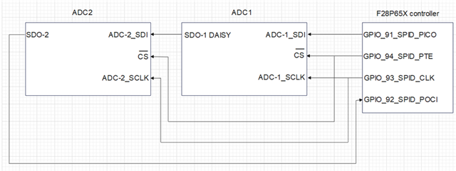
Thanks in advance for your support.

Best regards,

Divyesh Patel


  • Hello Divyesh Patel,

    The default mode of the ADS127L21 after power-up reset is dual SDO/DRDY mode.  In this mode, you cannot use daisy-chain.  In order to write to each of the ADC's in the chain, you must repeat the write to the FILTER3 register to reconfigure each ADC.

    Another customer recently ran into this same issue; please see the following e2e thread that describes exactly how to configure the ADC after reset.

     https://e2e.ti.com/support/data-converters-group/data-converters/f/data-converters-forum/1546195/ads127l21-daisy-chain-connection 

    Regarding the DRDY, you need to synchronize all ADCs in the daisy-chain using a common START signal, either using the START pin or by command.  Once the ADCs are synchronized, the DRDY pins on all ADCs will be synchronized, and you only need to monitor 1 DRDY pin for the entire daisy-chain.  Details for synchronization can be found in 7.4.6 of the datasheet.

    Additional guidance when using daisy-chain can be found in the following application note.

    ADS127L11 in Simultaneous-Sampling Systems

    Regards,
    Keith Nicholas
    Precision ADC Applications

  • Hello Keith,

    Thank you for your detailed answer and for pointing me to the related E2E thread. I have already reviewed almost all of the discussions related to the ADS127L21 and other precision ADC topics.

    As per your suggestion, I understand that after a reset, we need to reconfigure the FILTER3 register for each ADC in the daisy-chain. I am already performing this step in my code. However, I am still facing the same issue — both frames are returning 0x000000FFFFFF.

    If possible, could you please share any example code, register write sequence, or any of controller logic for configuring the ADS127L21 in daisy-chain mode? Having a working reference implementation would be extremely helpful for verifying my setup and resolving the issue.

    Please let me know if you require any additional details about my hardware connections, initialization sequence, or test conditions.

    Regards,
    Divyesh Patel

  • Hello Divyesh,

    We have generic example code, but it does not have any daisy-chain examples.  You can find the code at this link:

    https://www.ti.com/tool/download/ADS127L21-C-EXAMPLE-CODE

    I use the same logic analyzer/software; starting immediately after reset with default register values, please send a full *.sal capture file that shows the entire initialization sequence.

    Also, please make sure the /RESET pin is held high (either through GPIO control or tied to IOVDD).  Also, if you want conversion results, then either the START pin needs to be high, or you need to send the START command by writing to the CONTROL register START bit.

    Also, a screenshot of your schematic that shows the ADS127L21 connections would also be helpful.

    Regards,
    Keith

  • As you requested, I have attached the *.sal files for reference.

    I am holding the RESET pin high and manually providing the required delay (td-RSSC = 10,000 × CLKIN periods).
    In the first .sal file, you can clearly see that after the START pin goes low, the reset recovery time (~20 ms) is present in the logic trace.
    Only after this delay do I write the registers, and in this case I am able to read valid values such as 0x000000FFFFFF (i.e. the MISO line is not stuck at zero).

    However, if I do not add this manual delay after releasing RESET, then I always receive 0x00 on the MISO pin.

    The same issue occurs when I try performing a reset by SPI register write, or a reset by SPI input pattern — in both of these cases, the MISO output also remains stuck at 0x00 (this can be seen in the second .sal file).

    So at the moment I’m stuck — I am not getting any updated data on the MISO pin..

    In the following E2E thread, it was mentioned that you successfully wrote the FILTER3 (0x0B) register in a four-ADC daisy-chain:
    https://e2e.ti.com/support/data-converters-group/data-converters/f/data-converters-forum/1546195/ads127l21-daisy-chain-connection

    If you could please share the controller logic or example function you used to perform this would allow me to confirm whether my write sequence is correct, or if something is missing.

      5428.data.zip

    Thank you in advance!

  • Hi Divyesh Patel,

    Keith is out of the office right now, I will help in the meantime

    Is your controller latching the SDO on the correct (falling) edge? It looks like the last SCLK transition in the first 24-bit command comes right as DOUT is transitioning low to high. This is incorrectly being interpreted as a 1 when instead it should be a zero. The logic analyzer is also launching on the wrong edge in the "reset via SPI register" .sal file

    Also, can you confirm that you have 2 or 4 ADCs in the chain?

    Finally, SCLK must idle low for the ADC to function properly. There are glitches on your signals before your start trying to change the FILTER3 register where CS is being briefly brought low and SCLK is high. Please correct this behavior.

    -Bryan