DAC8742H: External reference input for DAC8742H

Part Number: DAC8742H
Other Parts Discussed in Thread: DAC8830, , TPS3840, TL431, DAC8740H

Tool/software:

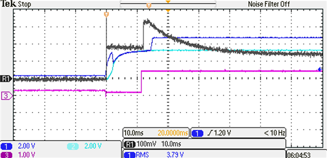
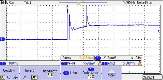
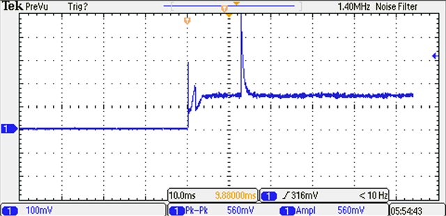
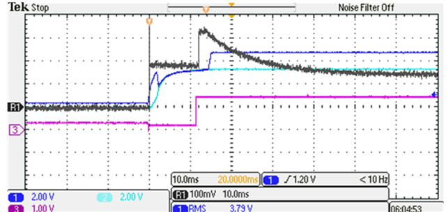
My MOD_OUT signal get distorted when changing from using internal (blue) to external (black) reference.(REF_EN was selected accordingly)

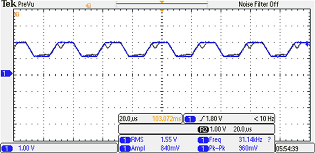
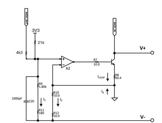
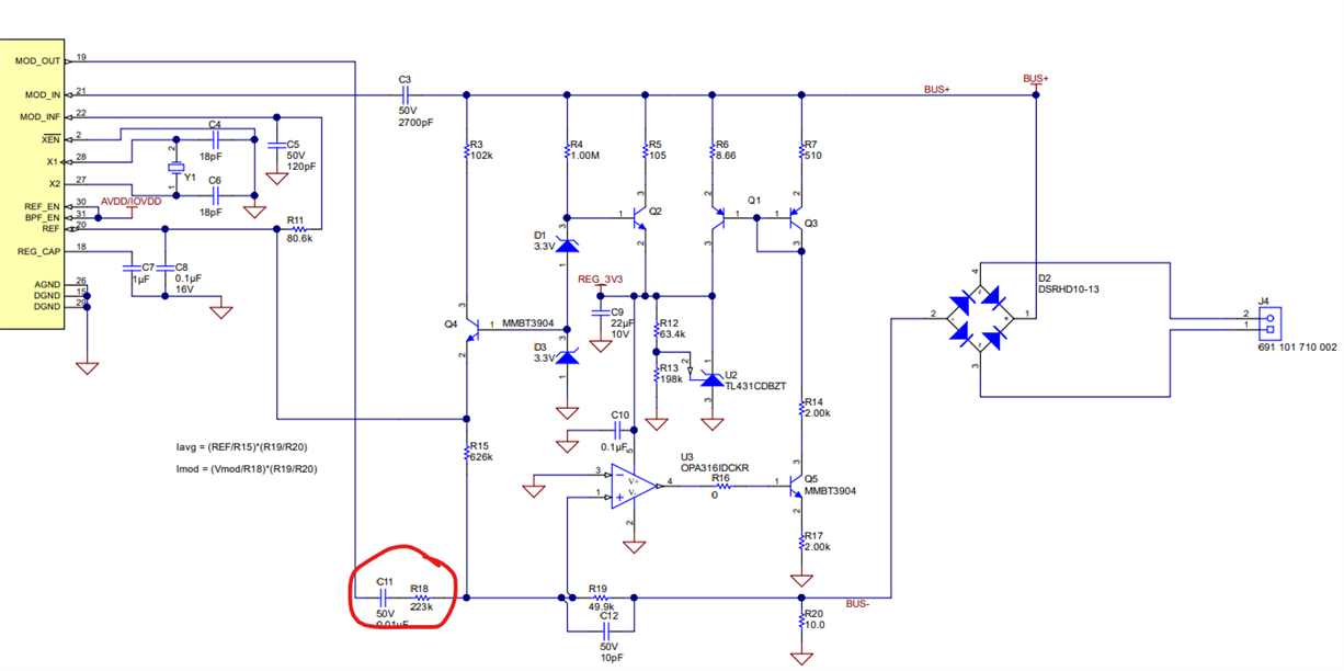
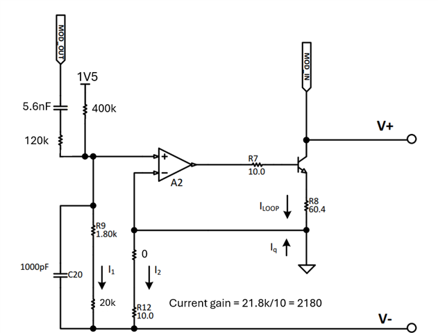
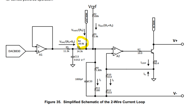
The MOD_OUT signal drive the 2-wire current loop circuit as suggesting in the DAC8742H datasheet

When I disconnect the MOD_OUT from the 2-wire current loop circuit (remove R4), the MOD_OUT  signal is OK with external ref

When I reduce the FF current by increase R4, the MOD_OUT  signal is OK with external ref

When I increase the input external ref, from 2V5 to 3V3, the signal was also OK with external ref

So my questions are:

  1. More details about the external reference internal electrical characteristic (max/min input current,  input impedance) 
  2. Any specific case where we should only use external ref
  3. Will the chip damaged if I use 3V3 for the external ref

  • Thong,


    I'm not sure what is causing the signal distortion. To me it looks like a bit of an oscillation, but I would have expected some overshoot if that's really the case. I would still use an oscilloscope to look at the reference input just to be sure. It's also possible that this is part of a loop oscillation, and you might be able to lower or increase the oscillation with changes to the capacitance at the V+/V- terminals. Regardless, I do have a couple of questions and comments for you about this schematic.

    First, what op amp are you using for A1 and A2? Are you using a DAC8830 to set the current? For the schematic shown in the data sheet, this Vref is not the same reference as used for the DAC8742H. This Vref is used as the reference for the DAC8830. It's not as clear in Figure 35, but it is shown on the previous page (30) in Figure 34. In in both figures, the Vref is also going to the 100kΩ + 2.4kΩ that sets up the lower limit current of 4mA for the loop. This reference is not used for the DAC8742H.

    As for your questions:

    1. I'll need to check on the external reference characteristics. I don't have any detail available. I don't think that the VREF pin would create a large load on the external reference. The data sheet says that the typical input current would be 4.5uA through different operation.

    2. I don't know of any cases where the external reference should only be used. I think for all the designs I've looked at, the internal reference is always used. I don't think I've seen a case where an external design was used.

    3. The device data sheet states specifically that the external reference should be between 2.375V and 2.625V. I don't think going over this value to 3.3V would cause damage to this device unless the supply voltage was below 3V.

    Again, I'm not sure what this distortion is. Can you provide a schematic for your system? 


    Joseph Wu

  • Hi Joe

    I did not use DAC8830 but just 3V3 to fix the DC current to about 15-16mA (this will never change in my application). So the schematic is like this. The op-am is  OPA335AIDR as recommended in the datasheet

    The reason for using the external reference is for the test case 5.1 in the Fieldbus Physical Layer Conformance Test which limit the current change to be under 1 mA per ms. Using the internal ref, I observed that the pin MOD_OUT jumping from 0 to 1.5V when the DAC8742 start up, causing a high charging current to the DC decoupling capacitor (C13=2.2uF in the  DAC8742HEVM Board Schematic)

    The black curve is the current drawing from the FF bus (through a 10 Ohm resistor), and pink is the voltage measured at the MOD_OUT pin. You see the MOD_OUT jump from 0 to 1.5V ( its idle state), causing a peak current that is not allowed by the Conformance Test. Have you experienced anything like this? And do you know any solution to soften this start up transition 

  • Thong,


    I think that when we had looked into this, we had some initial startup current issues as well, but from a different source. For us, it was more a problem with the microcontroller pulling too much current at startup. Our solution was to use a voltage supervisor to hold the reset of the mcu until after the loop current was established.

    If you use a 2.2uF capacitor at MOD_OUT, this large capacitance could certainly pull a lot of current when powering up to the loop. I did look at a schematic of something we tested. It looks like we used a significantly smaller capacitor of 0.01uF and a series resistance of 223kΩ. This should be much less current at the startup to settle at the loop. I'd mentioned this in your previous thread, but the schematic can be found in another post:

    https://e2e.ti.com/support/data-converters-group/data-converters/f/data-converters-forum/821316/dac8740h-the-reference-design-of-field-transmitter-with-profibus-pa 

    Joseph Wu

  • Hi Joe, thanks for this design. I see it uses a much higher current gain (~x5000) compared with the DAC8742HEVM (~x100), I will try this approach. 

    Also, it is another TI evaluation board that I can buy to test? or you just have the schematic. If I have to build it myself, do you have the BOM for it?

    Best regards

  • Thong,

    This is a board that we had worked with a third party to test FF capabilities. They had helped us develop the board and run the FF verification tests. In your previous thread, the notes on this board were what I pulled from to help answer your questions. It's not available from TI.com as this was just our test board.

    You've seen the schematic, let me see what else is available. I should be able to find a BOM.

    Joseph Wu

  • Thong,

    I was able to find the BOM for the circuit. It's in an Excel format. Read through it and let me know if you have any questions.

    Digi-Key Bill of Materials-DAC8740H_PAFF(001).xls

    Joseph Wu

  • Thank you very much Joe, I will use this reference for my testing 

  • Hi again Joe

    I keep using the suggested circuit in the DAC8742H datasheet, but tried to reduce the DC decoupling cap at MOD_OUT from 2.2uF to 5.6nF and use a series resistance of 120kΩ (see other value below). Then I have to increase the current gain to get the desired FF current. This should be much less current to charge the MOD_OUT cap, but due to the higher gain, I still get a similar current peak drawn from FF bus when MOD_OUT increase from 0 to 1.5V


    This is the current drawn from the FF bus through a 10Ohm resistor. Seems like the DAC8742 takes around 12ms to start up

    I am not sure if the new schematic solve this problem because the current gain circuit looks similar. Could you please share the startup current measurement of the new schematic, just to check if you have any glitch at around 12ms

    Thank you very much

  • Thong,

    Give me a couple of days to look this up. I haven't seen any scope shots on this and the only mention about start up issues involved the processor startup and the need for some power supervisors to hold the processors in reset. 

    Joseph Wu

  • Hi Joe, Do you have time to check it? I have just built the new circuit that you recommended. I still get a peak at around 12ms. There are also several rapid changes at the beginning that I believe not be allowed by the Conformance Test neither. 

  • Thong,


    I did find something in a report on the test results and it looks similar to what you have seen for the current spike at startup. Here's the scope shot that I found:

    The failure was for Maximum Current, Test 5.2.5, with RS=10Ω, and VBUS=32V. This looks almost exactly as what you've seen with a spike of current at about 13ms into the startup. The device passed Test 5.2.8 which was for the same test with a VBUS=9V. In the test, the supply current drawn, maximum, between 500us and 20ms after power up was 43.6mA (with 36.0mA maximum as the specification - 20mA + 16mA). At VBUS=9V the maximum current was measured to be 31.8mA, which was within spec.

    The original designer that designed the circuit left the group, and his only comment on this was that "To meet startup current specification voltage supervisors should be added to hold the reset pins of both MCUs low until the loop current is established. The team has recommended TPS3840. There is no specification on how quickly the device must communicate so several hundred ms is okay". Based on what I've seen, he thought this was the actual issue. If this current spike doesn't come from the setup of the MCU, I'm not absolutely sure where it comes from.

    My original thought was that if was the DAC8740H internal regulator was filling its capacitance REG_CAP. If that is the case, I would try to reduce REG_CAP C7 to 0.1uF. Another candidate would be the current used to fill up capacitance for the LDO start up. In that case, I would look to reduce C9 at the TL431 (22uF) by an order of magnitude just to see if this changes the startup.

    I'll see if there are any other notes on this startup problem. I had to do some digging to find this.


    Joseph Wu

  • Hi Joe, it is good that we have the same measurement. The current spike at 12-13ms, as I said before, is from the MOD_OUT pin when it reaches its idle state of 1.5V from 0V(pink curve). This is not relevant to the micro controller power consumption. 


    The MOD_OUT pin is controlled by the DAC8742. I guess when the DAC8742 start up, it takes around 12ms to set the MOD_OUT pin to 1.5V. Is there anyway to make this transition smoother ?


  • Thong,

    Ok, give me some time to look this over a bit. Out of curiosity, have you tried reducing the current gain? I know you increased the current gain to get the desired FF current, but I would expect that you could also lower the 120kΩ and 400kΩ resistor to compensate.

    Also, did you try checking the current at 9V? As I mentioned, our circuit passed this part of the test. However, I would expect that to have failed as well based on the source of the current.

    Joseph Wu

  • Thong,


    I've thought about this some more, and I don't think that my original idea of reducing the current gain will work. In the end, I think if you scale all of the resistors, the currents stay the same, and you have the same result as before. I still think it's worth testing the system at 9V supply. I would have thought this would also give the same result, but ours did show a smaller current which did pass the test.

    However, there is something that I wanted to point out. For the maximum rate of change of quiescent current, the specification is that the change should be less than 1mA/ms. However, this specification for test 5.1.6 (5.1.11 for 9V operation) is limited to any point in the waveform from 20ms after power is applied.

    So in this case:

    the test does not pass because, the settling tail does continue past the 20ms, and does look like the change in current is still a little high. However, in the following plot:

    the test passes because the current has settled by the time 20ms after the power has occurred. There are similar tests that measure the change in current vs time during the reception of the DUT, and they may also be limited to 20ms. The tests seem to pass on our board based on what I've seen.

    In the other test, for 5.2.5 (5.2.8 for 9V operation) the IDUT_MAX should be less than IDUT+20mA. In that case, the time interval should be 500us ≤ t ≤ 20ms. For that one, it looks like the first scope plot have passed that test because the spike is less than 20mA above the operating current. However,  the second one failed the test because the second spike is too high.

    I don't know if explaining these test results gives you any more clarity. I would assume that you would want to first solve the settling time first, and then try to reduce the spike magnitude second. 


    Joseph Wu