Tool/software:
Hello,
I think I'm experiencing same issue to related question.
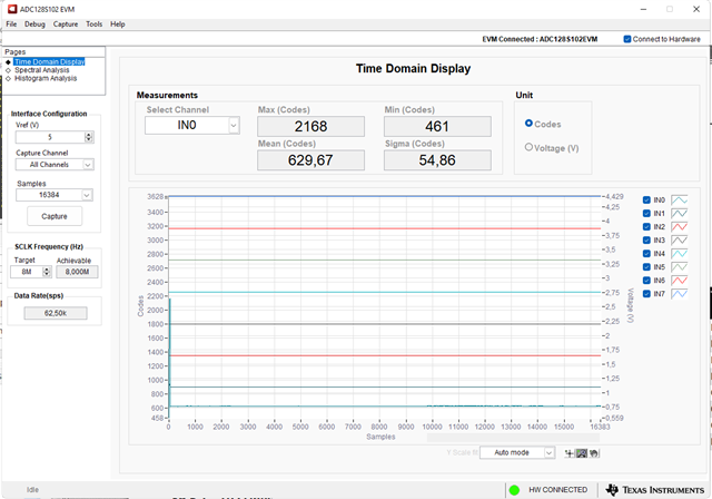
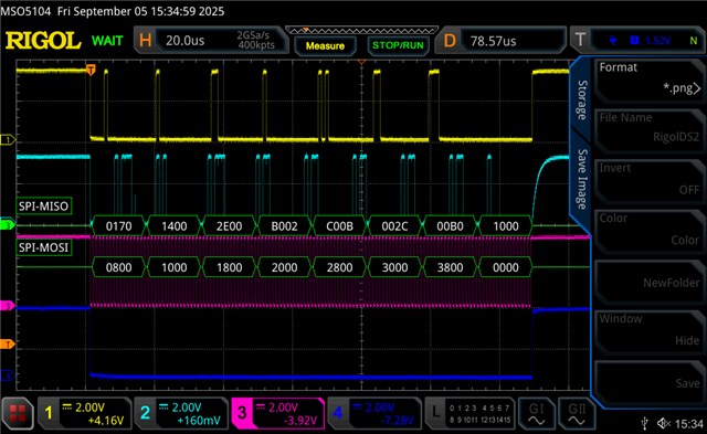
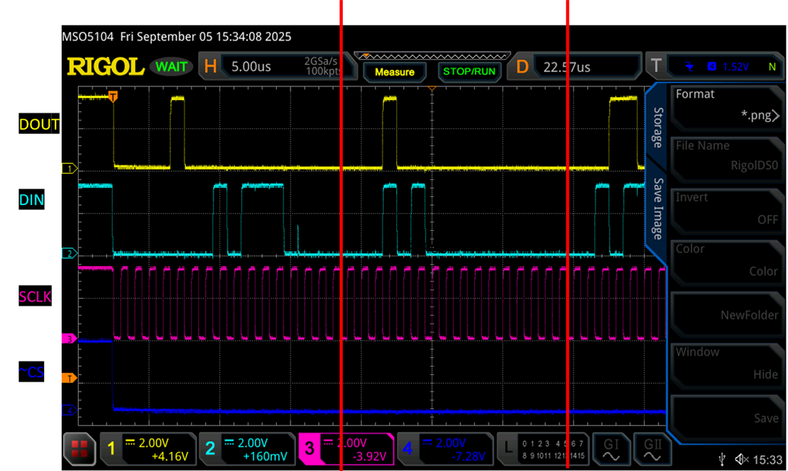
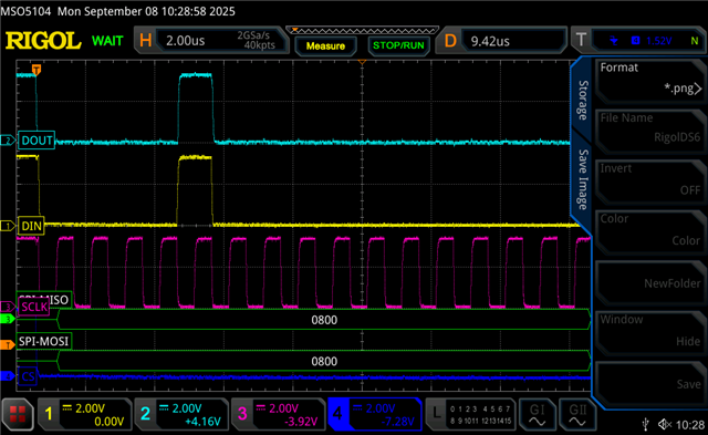
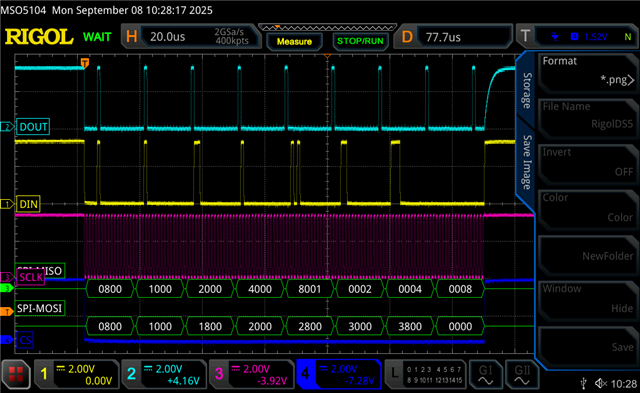
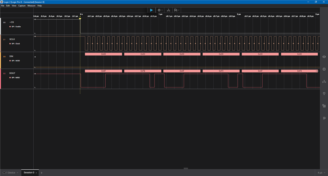
I think that everything is set correctly to retrive data in continuos mode. fSCLK set to 2 MHz, SPI mode 3.
But the data from channel 1 to 7 are never the same even if I put the some resistor (with different value) on input channels.
I'm using ADC128102EVM connected to Microchip SAMRH71 microcontroller.
Do you have any suggestion to understand if there is some SPI configuration error?
Thanks and regards,
Enrico
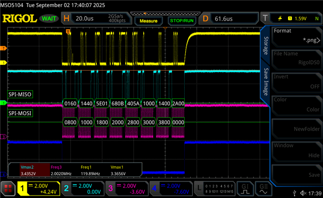
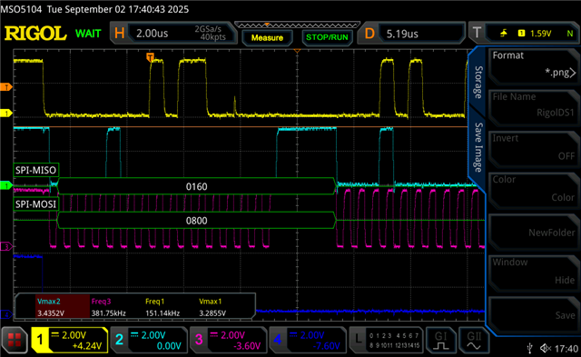
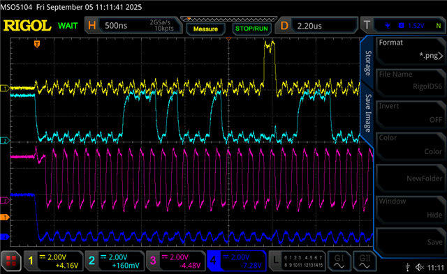
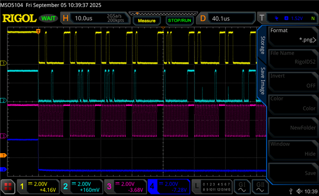
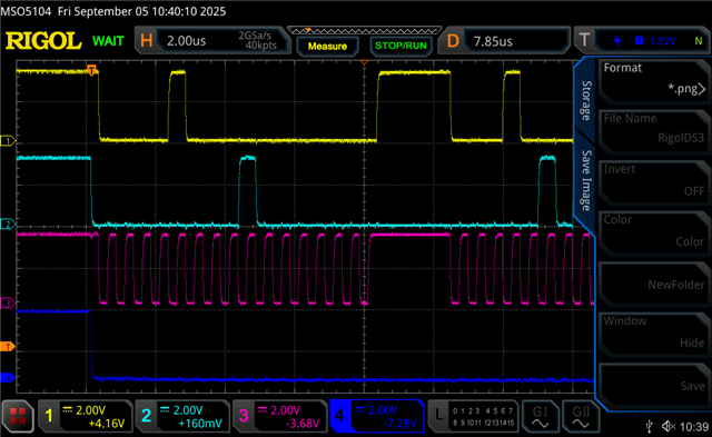
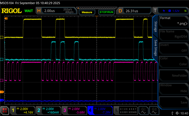
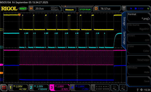
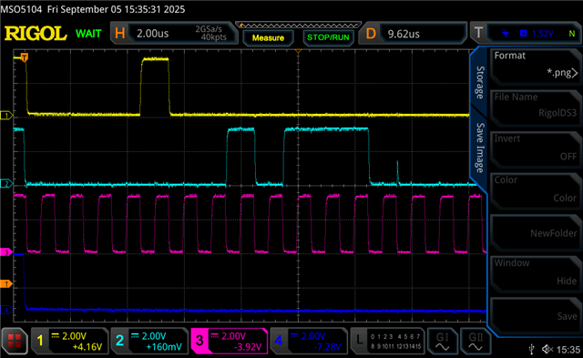
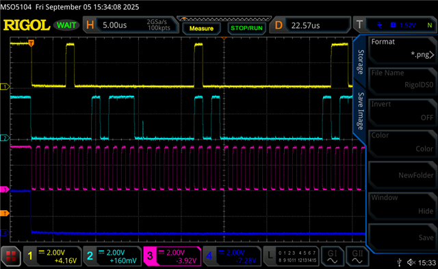
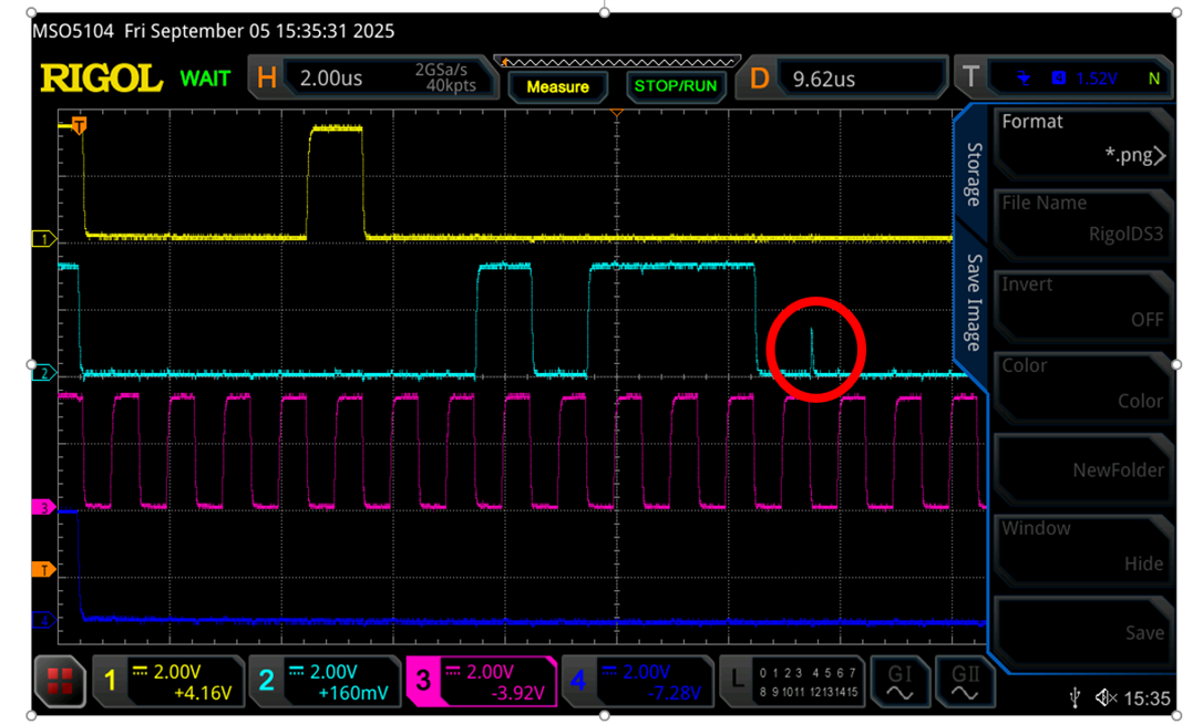
Yellow: MISO
Light Blue: MOSI
Purple: CLK
Blue: CS