DAC5672A: Interleaved mode acccess

Part Number: DAC5672A
Other Parts Discussed in Thread: DAC5652, DAC5672, DAC5662

Tool/software:

Hi,
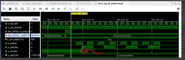
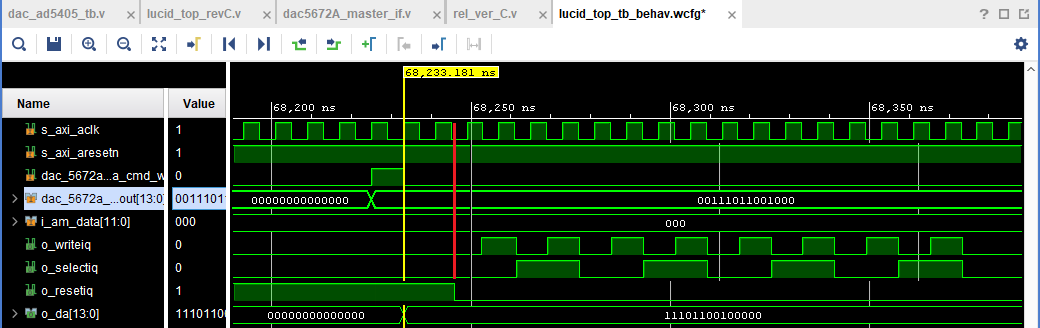
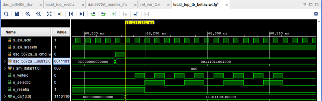
I’m trying to work with DAC5672A in Interleaved mode.
I’m writing the same data to both channels.

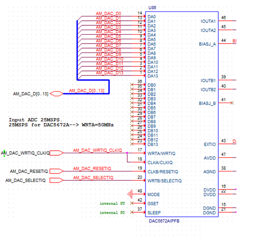
WRTIQ and CLKIQ are connected to the same line.

As I understand it, on the fourth rising edge of WRTIQ and CLKIQ, the data should enter.

After it didn’t work for me, I added 4 more clock cycles, but even now it’s not functioning correctly.
What is the issue?

Did I understand it wrong?

I also used below document (DAC5652, DAC5662 and DAC5672 Interleaved Data Mode).


dac5672a_X2_Interleaved_Mode .pdf

Thank you

Gil

  • Hi Gil,

    How is the WRTIQ and CLKIQ pins being driven? Meaning what is the source? Do you have enough signal amplitude? What frequency?

    Regards,

    Rob

  • Hi Rob,

    WRTIQ and CLKIQ are 62.5MHz signals driven by an ARTIX 7 FPGA.

    Measuring on WRTIQ and CLKIQ pins give VIL=0.23V(max), VIH=3.14V(min).

    When we access the device as you see in the first message,  a "single transaction" access, we don't see the required voltage.

    When we perform a continues access to the device (continuously writing the same data, i.e. toggling WRTIQ/CLKIQ/SELECTIQ with the same data), it outputs the required voltage after some time (I don't know how many cycles it takes to achieve that).

    We assume a single transaction access is required to change the DACs output. No need to continuously writing to it.

    Is anything logically wrong with the transaction you see in the first message?

    thanks,

    Gil

  • Hi Gil,

    Yes, you only need to write the spi registers once after the device is powered up.

    Measuring on WRTIQ and CLKIQ pins give VIL=0.23V(max), VIH=3.14V(min).

    Where is this being measured? Make sure you are measuring at the DAC clock pins.

    On the ILA I see your ResetIQ should be with the falling edge of the SelectIQ. Can you try delaying it to the right? See below.

    Regards,

    Rob

  • Hi Rob,

    WRTIQ and CLKIQ are measured, of-course, on the DAC5672A pins.

    I sent your comment to our FPGA guy.

    Another issue (maybe both are related):

    We see a spur or some kind of a small "hill" at around 17.4KHz at -68dBm on the DAC5672A outputs (it is measured on the OPAMP output that is connected to the DAC5672A output, see drawing).

    Both OPAMPS outputs show it (A and B). 

    It gets stronger as the DAC5672A output gets higher (the below picture shows it with DAC5672A digital input at maximum, around 0.5V at its output and 2V at the opamp output).

    It cannot be seen by scope since the voltage is around 400uVpp.

    Still, it appears on our product output and we need to eliminate it (it modulates into the signal output).

    It does not come from the DAC5672A power supplies (inspected AVDD) and not from the OPAMP (disconnected the OPAMP and inspected the DAC5672A output to find it at around -78dBm).

    It seems the DAC5672A is the source. Are you familiar with that? How do we eliminate it?

    thanks,

    Gil

  • Hi Gil,

    Are you using any power supplies switchers on the board? Before the LDO?

    What is the switching frequency?

    Where are they located?

    Regards,

    Rob

  • Hi Rob,

    As i wrote, I checked the power supply of the dac5672a: i don't see this spur on the device AVDD. The spur seems to come from within the device.

    It's a 17.4KHz spur.

    DC2DC switch in much higher frequencies.

    Is there some internal mechanism, in the device, that can create it?

    It gets higher with the DAC5672A output.

    Thanks,

    Gil

  • Hi Gil,

    There is no mechanism that would create a 17kHz spur within the DAC.

    My guess is something is coupling and it doesn't have to originate from the AVDD. It could be other power supply domains.

    I assume you are using one ground?

    Can you see the spur when the output is disconnected from the amplifier? When the both the outputs are just terminated?

    If you are using a spec analyzer to check this, since it is 50ohms. You will need to change the termination to reflect below.

    Otherwise, the output is lopsided.

    Regards,

    Rob

  • Hi Rob,

    The 17.4KHz issue is solved.

    The EVB schematic has a 0.1uF capacitor in parallel to the BIASJ_A resistor, and there is a comment not to assemble it.

    This is the culprit.

    You can see below the energy around 2*17.4K, 3*17.4K, 4*17.4K (opamp output in my circuit).

    In the picture below the capacitor is not assembled:

    When it is assembled (my case), it affects the internal circuitry that creates the 20mA (IFS) out of the 1.2V (doesn't matter if internal or external) and/or the internal two control amplifiers and/or the circuitry that drives Iout, in a way that creates the 17.4KHz disturbance we see.

    We are still left with the interleaved mode access which does not work:

    The FPGA guy input your remark (ResetIQ should be with the falling edge of the SelectIQ), but it still does not work.

    What are we missing here?

    thanks,

    Gil

  • Hi Gil,

    Looking into this further. 

    Meanwhile, can you please check the rest of your board to make sure it has been properly assembled?

    Thanks,

    Rob

  • Hi Rob,

    The DAC5672A is assembled as you see in the schematic picture I attached.

    The only correction to be made was the capacitor.

    Input bus and controls are as shown in the picture.

    I will say that dual bus mode access works fine (I utilize only DACA bus and disconnect the mode pin from GND).

    However, we need the interleave mode.

    thanks,

    Gil

  • Hi Gil,

    Also, please send some example output spectrums with the test conditions and setup, so we understand what is not working in IL mode.

    I see you are using the Artix 7 for the sampling clock at 62.5MHz.

    Regards,

    Rob

  • Hi Rob,

    We sent you the screenshot from the ILA.

    These are the controls presented to the DAC5672A.

    When I send data to the DAC so it outputs it as voltage, I need to perform these transaction twice before the voltage is updated on the DAC outputs.

    What else can I send you?

    thanks,

    Gil

  • Hi Gil,

    I think Rob was asking for frequency spectrum. Are you just looking at DC output? From the ILA screenshot above it seems like you are just updating from 0x000 to some other constant pattern, so a voltage shift alone.

    I've taken a look at this also and am wondering if the issue is due to reset_iq dropping while the clk is rising edge, and some timing is not being met such that you lose the entire first data word update. If you drop reset_iq on a falling clock edge like I show below in a modified version of your ILA, does this make the output update on the first transaction? Is that the problem here? If not I am not following what the exact issue is. 

    Thanks, Chase

  • Hi Chase, Rob,

    Why do you need frequency spectrum? (SA).

    I used it since we had a very low disturbance (less than 1mV) which cannot be detected by scope and ideal to be tested using a SA.

    For the issue we now have, writing doesn't work (a digital/logical issue), a scope is the proper instrument. Do you disagree?

    In our case, I am looking just for a DC output, once I input the command to create it.

    The DAC will also be used to create a continuous signal, but this is for a later stage.

    You are correct. The problem is the output doesn't update on the first transaction (only on the 2nd).

    We do drop resetiq on the falling edge of clockiq (in our design clkiq and wrtiq are shorted).

    (you probably mistaken clkiq with axi_aclk which is an internal fpga AXI signal).

    So, we do everything as in the datasheet and the DAC5672 Interleaved Data Mode document, and it still doesn't work.

    What are we missing here?

    Thank you

    Gil

  • Hi Gil,

    Can you please send us an updated snapshot of your ILA?

    Also, please trying shifting SelectIQ to be high before first rising edge of the WriteIQ/CLKIQ.

    Regards,

    Rob