This thread has been locked.

If you have a related question, please click the "Ask a related question" button in the top right corner. The newly created question will be automatically linked to this question.

ADC32RF55: ADC32RF55 Register Write/Read Problems

Part Number: ADC32RF55
Other Parts Discussed in Thread: , ADS54J40, LMK04828, LMK04832

Hello,

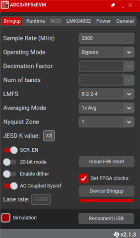
I'm testing with the ADC32RF55.
I extracted the ADC registers from the ADC3xRF5xEVM and configured them, but I'm not getting any output from the FPGA's TI-204C-IP.
So I tried reading the ADC registers, but it seems they weren't written correctly. Even if I write to each register individually and then read it back again, the write operation still fails.

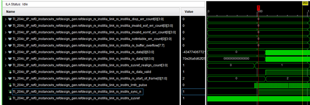
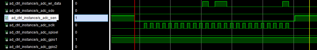
The picture below captures the SPI signals, GPIO1,2, and SPI SEL during Write/Read using the FPGA's ILA (Internal Logic Analyzer).

I checked the power supply to the ADC. I also reset it before writing the register. SPI clk is 5MHz.

Why can't I read the register?


<Write : address 0x02C, data 0x01>

write_2c_01.png

<Read : address 0x02C>

read_2c.png

Best Regards

Cho

  • Hello,

    The register setting and register reading issues have been resolved. It seems that the delay was the problem.

    When I read address 0x298, it reads as 0x1E. Does this mean that the calibration was successful?

    However, when I check the ILA results connected to the TI-204C-IP on the FPGA side, the output is not correct. What should I check in this case?

    Best Regards

    Cho

  • Hi Cho,

    Per the datasheet: The status of the calibration can be read back from register 0x298 (CALIBRATION page). Successful calibration reads back 0x0E on the 4 LSB of that register.

    Are you sure you are reading the 4LSB of the register?

    Regards,

    Rob

  • Yes, 0x1E means calibration is successful.

  • Hello Chase,

    I have an ILA (Initial Lane Alignment) problem between my ADC and my TI-204C-IP.

    As shown in the figure below, when the FPGA IP is in TX/RX loopback mode, "rx_sync_n" changes to high and the serdes output is also correct.

    <loopback mode ILA >

    However, during the ILA process of ADC, rx_sync_n does not become high.

    <ADC-FPGA ILA>

    After completing the ADC settings, I read the address 0x298 and checked that the value output as 0x1E was successfully completed to confirm that the calibration was completed successfully.

    The output of TI-204C-IP, "rx_sync_n" is connected to GPIO1 of ADC.

    In "jesd_link_params.vh" of IP, ADC_RESOUTION is set to 16. Should I change this to 14?

    Please help me with what other things to check.

    Best Regards

    Cho

  • Is the physical net changing any voltage? Leaving resolution as 16 is ok because your data would just be incorrectly parsed, ie 14 bit sample, then it's 2 LSB would be the 2 padded 0's. This is assuming LMFS=8224. Still, this would not prevent link from coming up.

    If you restrict to one JESD lane does SYNC toggle at all? Lane polarity does not matter for 8b10b CGS and ILAS so those are less important for now.

    Seeing that SYNCb never even toggles low, this seems like you have the wrong IO mapped on your FPGA, or there is a strong pullup which your FPGA cannot sink to logic low.

    This is a custom board or using the ADC32RF55EVM?

    Chase

  • Hello Chase,

    This is a custom board. However, I recently developed a design using the ADS54J40, the same FPGA. This time, I changed the ADC to the ADC32RF55. The circuit and PCB are very similar to those I developed previously. However, I am continuing to verify the design, keeping in mind the possibility of hardware issues.

    There is no pull-up between FPGA IO and ADC GPIO1. When tested in TX/RX "loopback mode" using TI-204C-IP, rx_sync_n goes high and also something is output from Serdes. 

    I know that it is possible to set the /sync signal using register settings via SPI.(address 0x21 in the JESD page)

    So I changed the settings so that TI-IP's output signal "rx_sync_n" does not output to GPIO1 of the ADC and tried to sync via SPI.

    However, rx_sync_n is still not high and the monitoring signals and Serdes outputs connected inside the TI-IP are 0.

    If the rx_sync_n signal in the TI-IP does not go high, does that mean the ILA(Initial Lane Alignment) has failed?

    What else should I check?

    Best Regards

    Cho

  • Hi Cho, here are some questions. I'm just trying to understand exactly where you're at so we can get you up and running quickly,

    • All of your ADC configuration is from the GUI?
    • I can generate a config and ensure the ADC is functional for you if needed but need details.
    • What sample rate?
    • What is the LMFS mode you are using?
    • What is application clock? I imagine this is ok since your fpga is running and can work in loopback. Is the loopback test serdes rates matching the ADC serdes rate?

    If I think of any more things then I will update this post. 

    Chase

  • Hi Chase,

    • After setting the registers in simulation mode in the ADC3xRF5xEVM GUI, extract the registers. Then, the extracted ADC register values ​​are set using the FPGA. At this time, the data order and delay values ​​extracted from the EVM GUI are applied as is.

    Here's what I've set up:  

    • Other settings include K=32, Scramble enable, etc.
    • The application clock supplied to the transceiver of TI-JESD-IP is 125 MHz, and the Sysref clock is 7.8125 MHz. I used LMK04828 to generate TI-204-IP's clock, ADC sampling clock, and Sysref clock. The frequency and quality of the clocks were checked with an oscilloscope and it was good.
    • And, In the loopback test, the Serdes rate and ADC Serdes rate matched each other. The lane speed was set to 5 Gbps.
    • I know that the rx_sync_n signal output from the TI-204C-IP is a signal to notify the start of CGS to the GPIO1 (/SYNC) of the ADC. If TI-204C-IP (JESD204B RX) receives K28.5 properly from ADC, rx_sync_n will change from low to high, right? Considering that the rx_sync_n value does not change from low to high, is the problem in the CGS phase?

    If you need any additional information or materials, please let me know. I can also provide relevant schematics and PCB layout information.

    Thank you for your help.

    Best Regards,

    Cho

  • Hi, Chase

    I tried setting the ADC sampling rate to 500MHz. Both the CGS and ILA processes proceeded OK, and Serdes output was also generated.

    Of course, the clock outputs of LMK04828 and the line rate(2.5Gbps) of the transceiver and the free-running and DRP clocks (62.5 MHz->31.25MHz) of TI-204C-IP were also changed at this time.

    Again, I tried changing the ADC sampling rate to 1GHz and changing the LMK04828 output clock, TI-204C-IP transceiver settings, etc., but the TI-204C-IP output rx_sync_n does not go high and it does not seem to pass the CGS process.

    I'm concerned about the levels and offsets of the CLKP/M and SYSREFP/M signals input to the ADC.
    For my current testing, I've set the LMK04828's CLKP/M and SYSREFP/M outputs to LVPECL. I've attached the relevant schematic. Could you please review it?  ADC32RF55EVM does not use LMK04828, and the sampling clock and sysref input range of ADC32RF55 seem to be different from those of ADS54J40.

    4705.ADC32RF55_LMK04828.pdf

    Best Regards,

    Cho

  • Hi Cho,

    This is odd that you can get CGS and ILAS at the lower rate but not at the higher sample rate. I know customers have used LMK04828 or LMK04832 in the past to clock the ADC in LVPECL2000mV mode before and it was functional. This is the same configuration like you have. Are you able to see the PLL2 lock on the LMK? I imagine you left the configuration the same and simply adjusted the output divider. This would build confidence in the clocking.

    I would check that R166 is not populated, it shouldn't be needed as there is an internal 100ohm termination.

    The ADC has some slightly different register configs for different sample rates, but this won't prevent the link from coming up. I think this is pointing to FPGA not meeting the timing.

      can you look into this and provide your thoughts?

    Thanks, Chase

  • Hi Cho,

    Please confirm if you have configured the TI JESD IP to have a transceiver data width of 32 bits. In your initial design, the SERDES rate is 2.5Gbps and the reference clocks are 62.5MHz. 

    In addition, please send us the details of the changes that you are making to the JESD IP when moving from the 500MHz design to the 1GHz design.

    Regards,
    Ameet

  • Hi Chase,

    I can check the PLL2 lock in LMK. After controlling LMK, the PPL2 lock LED lights up.

    I also removed the R166, 100ohm termination resistor, but the result is the same.

    I left the LMK settings as they were and just adjusted the output divider.

    At 500MHz sampling, I verified that both LMFS 8-2-2-4 and LMFS 8-2-8-20 pass the CGS/ILA process and produce serdes output.

    However, when sampling at 1GHz, the output signal rx_sync_n of TI-204C-IP does not go high. I guess this means that CGS is not working?

    Is it an FPGA problem or a PCB problem?

    Best Regards

    Cho

  • Hello  Ameet Bagwe,

    The changes made when setting from 500M to 1G are as follows.

    And the transceiver settings in 1G are as shown below.

    First, I set the 984 registers below extracted from the GUI, including the delay time.

    SIM_DUAL_ADC.write(0x000,0x01)
    SIM_DUAL_ADC.delay(0.1)
    SIM_DUAL_ADC.write(0x000,0x00)
    SIM_DUAL_ADC.write(0x001,0x00)
    SIM_DUAL_ADC.write(0x009,0x20)

    .......................omission.........................

    SIM_DUAL_ADC.write(0x058,0x3F)
    SIM_DUAL_ADC.write(0x0FE,0x00)
    SIM_DUAL_ADC.write(0x0FF,0x00)
    SIM_DUAL_ADC.write(0x045,0x8A)
    SIM_DUAL_ADC.write(0x045,0x0A)
    SIM_DUAL_ADC.delay(3.9000000000000004)

    Second, JESD Interface Synchronization Using SPI Writes

    SIM_DUAL_ADC.write(0x005,0x04-- Select JESD page
    SIM_DUAL_ADC.write(0x021,0x41-- Configure ADC to Control SYNC using SPI writes
    SIM_DUAL_ADC.write(0x021,0x61) -- Configure JESD interface to send K28.5 for receiver synchronization

    Third, TI-204C-IP's  rx_sync_reset RUN 1->0 . In normal case, "rx_sync_n" transitions from low to high.(in case of 500M, it works.)

    Send rx_sync_n to ADC_GPIO1 through the FPGA's output pin

    Fourth, send normal ADC Data.

    SIM_DUAL_ADC.write(0x021,0x41) -- Configure JESD interface to send normal ADC data

    Please check that my settings and operating sequence are correct. I'm worried there might be a problem with the board. I hope it's not the board.

    Best Regards,

    Cho

  • Cho, can you send me your full schematic perhaps for me to look at this a bit more? I will send you an email which you can reply to so be on the lookout for that please.

    Thanks, Chase

  • Hi Cho,

    I will recommend updating the sys clock frequencies. The suggestion is to set sys clock to Line Rate / 80. For 2.5Gbps, it should be 31.25MHz. For 5Gbps, it should be 62.5MHz. Setting it to a higher frequency is not a problem (as long as timing closure passes), but you will see the lane data valid signal going low to account for the overall data rate. 

    If the SYNCn signal never goes to '1', this will usually mean that the ADC (Tx) and FPGA (Rx) are not set to the same SERDES rate. Alternatively, it could mean that the FPGA SERDES PLLs have locked. Please confirm if you see PLL locked output set to '11' (one locked signal for each Quad).

    Regards,
    Ameet 

  • Hi Cho,

    The only concern with the board is the DVDD copper plane on layer PWR2. The thickness shows 0.018mm which is for 1/2oz copper. At the 2mm width track/copper pour for the power rail, I am worried at higher sample rate (and thus higher power consumption), this DVDD plane has higher IR drop and may be browning-out at the device. I would recommend doubling this width in your next redesign if applicable just for improved IR performance here.

    Can you probe one of the DVDD voltage at the ADC capacitor before/after programming at the successful sample rate and also at the higher, failing sample rate? I'm curious if there is any difference here. If there is no difference you are probably ok since the 5A LDO you chose is a good choice.

    I think perhaps moving to a signal integrity test would be the next steps. This would mean implementing PRBS pattern on FPGA to confirm that your board material (shown as FR4 alone) is not degrading serdes signal integrity. FR4 should be ok for this device but closer to 13Gbps serdes rate may be pushing the capabilities perhaps. PRBS testing will help to further investigation in the right place.

    Attached is also a configuration which I have tested on hardware and should be sufficient to test 2.6GSPS in LMFS8224 mode if you wanted to compare this vs gui simulation result. Theoretically they should be identical and when I created the GUI and register sequence for simulation mode, I tested and confirmed they were the exact same, however there might be a mistake. I would advise to start with this configuration below just to eliminate one more variable.

    2p6GSPS_8224_ADC32RF55EVM.cfg

    Thanks, Chase

  • Hi chase,

    Thank you for reviewing the circuit. I observed the voltage drop of DVDD1.2V supplied to the ADC with an oscilloscope, but no abnormalities were found.

    I'm currently using the xcku040-ffva1156-1-c FPGA. The maximum line rate in the Ultrascale FPGA Transeivers Wizard (1.7) is 12.5 Gbps.

    So, Could you provide me the ADC configuration file for 1Gsps?

    I compared the settings file you sent me with the file extracted from the GUI simulation mode. The number of registers and the settings seem to be slightly different. The settings are as follows:

    Best Regards

    Cho

  • Hi Ameet,

    I changed sys_clock as you mentioned. But SYNCn signal never goes to '1'.

    At this time, only qpll0_locked is "11". qpll1_locked and cpll_locked are "00".  Is there any problem?

    Best Regards,

    Cho

  • Hi Cho,

    The design uses QPLL0 for both Quads, so this is fine. The only other possibility is that the Rx is not locking to the Tx, so this can mean one of two things:

    1> The ADC and FPGA are not set to the same SERDES rate
    2> There are signal integrity issues (lanes lock at 2.5Gbps, but not at 5Gbps)

    Please confirm if you have tried a signal integrity check using the ADC in PRBS mode (and the IBERT IP from Xilinx). 

    I also noticed that in your sequence you have not listed when the master_reset_n is set to 0 or 1. Kindly send me those details as well.

    Regards,
    Ameet

  • Hi Ameet,

    I'll try signal integrity testing using the ADC (and Xilinx's IBERT IP) in PRBS mode. I'll share detailed results once the tests are complete.

    The master_reset_n is connected directly to the external reset signal input to the FPGA.

    The external reset signal is generated using the TPS3840DL28DBVR. So when the board is powered up, master_reset_n is executed first. After that, master_reset_n is not executed.

    Should I execute master_reset_n(0->1) right before TI-204C-IP's rx_sync_reset RUN 1->0?

    Best Regsrds

    Cho

  • Hi Ameet,

    Let me tell you what I've been testing so far. 

    • ADC sampling is now possible up to 1500M. I ran some tests by gradually increasing the sampling clock of the ADC. 500Msps, 600Msps, 800Msps, 1Gsps, 1.2Gsps, 15Gsps, 2.4Gsps... . It seems that the CGS process does not work at 2.4Gsps. 
      • By modifying the master reset sequence of TI_204c_IP, it became possible to achieve speeds up to 1500Msps (Lane rate 7.5Gbps). 
      • Previously, master reset was performed by the FPGA's power on reset, but it was changed to perform master reset before rx_sync_reset.
      • The overall setup sequence is as follows:
        • ADC_Reset 
        • ADC Register Setting
        • master_reset_n
        • rx_sync_reset
    • Also, I checked the SI using IBERT IP. Tests were conducted at ADC sampling rates of 500M(Lane rate 2.5Gbps), 1500(Lane rate 7.5Gbps), and 2400M(Lane rate 12Gbps), respectively.

                And, When it is 2400Msps, IBERT status shows "No Link". There is no problem in IBERT's loopback mode. 

                Could it be lane's signal integrity problem?  Or is this issue caused by a clock synchronization issue with the LMK04828?

                Would it be worth testing by gradually increasing the sampling rate from 1500Msps?

    Best Regards

    Cho

  • Hi Ameet,

    I've added a few more tests.

    I'll create a new forum with the latest results.

    Best Regards

    Cho