This thread has been locked.

If you have a related question, please click the "Ask a related question" button in the top right corner. The newly created question will be automatically linked to this question.

ADS1299: ADS1299 Daisy Chain Not changing sampling rate

Part Number: ADS1299

I'm implementing 2 of the ADS1299 chips in a daisy chain configuration, like in figure 70 of the datasheet.  The Start, CLK, ~CS, SCLK, and MOSI are shared between the two chips, while the DOUT1 is wired to Daisy_In0 and DOUT0 is wired to MISO.  

I'm able to initialize and get readings out of the chips, but I'm finding that the sampling rate of the second ADS1299 doesn't change from the default (250SPS).  I've verified that the second ADS1299 is receiving commands because I can successfully change the gain.

Is there something that would cause this second chip to not respond to the rate change command?
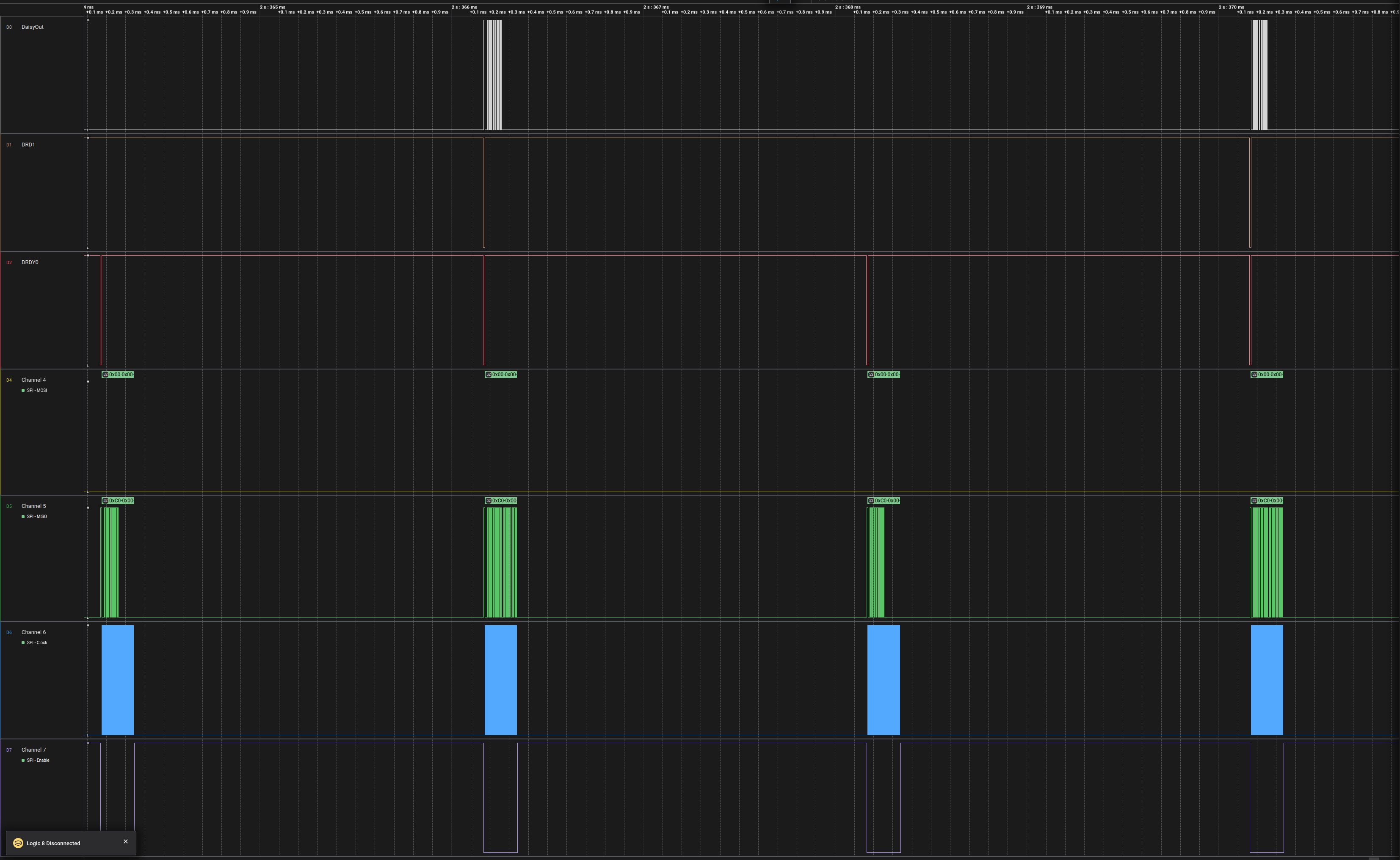
image.png

  • Hello Seth,

    Just to verify, what value are you reading from the CONFIG1 register at initialization from the first ADS1299, and what value are you trying to change the CONFIG1 register to? Additionally, is the sample rate of the first ADS1299 changing?

    Our device expert is out-of-office -- please expect a response the week of 2/27.

    Regards,

    Payton

  • Hello Payton,

    I'm writing 0xB5 (181), and have confirmed I'm reading that back as well, but only from the first ADS1299.  This should be setting it to Daisy Chain mode, Oscillator Output (to sync the two chips, as one has CLKSEL=0 and the other CLKSEL=1), and output data rate of 500SPS.  One thing I noticed is that when I do a read register, the register value is not being output on the second ADS1229's DOUT pin.  With the Daisy Chain topology, is there intention that read registers aren't going to be needed? 

    Yes, the sample rate of the first ADS1299 is changing.  The 2nd and 3rd channel above (brown and red respectively), shows the DRDY lines of both chips.  Also, the 1st signal (white) is the DOUT->Daisy_In signal, so it's outputting data as expected, but at the default rate. 

    I've also tried power cycling the whole board to see if it latched up somehow, but hasn't cleared the issue.

    Thanks,
    Seth

  • Hello Payton,

    I'm following up to see if that device expert is back and can take a look at this issue.

    I've continued testing out the other functionality and this is the only thing holding me up.  

    Also, I can confirm that I'm seeing this behavior on all 4 boards that I've brought up, so it's thankfully consistent.

    Thanks,
    Seth

  • Hi Seth,

    Thank you for your patience. 

    Can you share a complete schematic showing the inputs and connections between both ADS1299 devices?

    Device 1 in the daisy-chain has no way of knowing if other devices are connected "upstream." Even systems with a single ADS1299 would use the device in "Daisy-Chain Mode" (/DAISY_EN = 0) by default. Can you disconnect DOUT1 from DAISY_IN0 and see if the DOUT1 pin toggles as expected when executing a register read command? Can you confirm the SDATAC command is being sent to both devices before making any register read/writes?

    Regards,

    Ryan

  • Hi Ryan,

    I've uploaded the schematic.  Please note that the inter-chip connections are made on the top sheet.  The various jumpers are to possibly configure the ADCs between Daisy Chain and standard-SPI modes. 

    I've verified that SDATAC is being sent out before doing any register read/writes.  The init procedure is:

    1. Hardware reset pulse.  (I have verified both chips are receiving it.)
    2. Send SDATAC. I've confirmed in software and also on the logic analyzer.  
    3. Write CONFIG1-3, CHxSET (1-8), BIAS reg (2x) LOFF reg (2x).  I've tried not setting any of these, but that doesn't fix it. 
    4. Read CONFIG1 as requested above.

    I noticed that the DOUT1 does not respond when the read register is sent.  You mentioned about disconnecting DAISY_IN0 and DOUT1.  Is there a reason to do this?  I'm seeing the DOUT1 sending data later when its DRDY goes low (as expected), so I would think there isn't a HW conflict happening there, right? (See screeshot for details)

    I've also verified that the CS line is consistent between the two chips. (It's wired together on the PCB through a jumper, but worth a sanity check)

    Thanks,
    Seth

    system.pdf

  • Hi Seth,

    True, I was wondering if there was a loading issue with the DOUT1 pin. The fact that it outputs conversion data but does not respond to RREG commands tells me that it might not be responding to the SDATAC command.

    Can you completely isolate Device 0 from Device 1 for now and try communicating with Device 1 alone? When you test register read/write commands, can you probe the logic analyzer directly at the input pins of U6?

    What is the SCLK frequency in your setup and how much time does it take to send the two-byte RREG command? 

    Regards,

    Ryan

  • Hi Ryan,

    I think the only way to truly completely isolate the devices would be to desolder Device 0.  I'd prefer to avoid that as I can't really spare a board right now. I did separate the devices using the jumpers available:  

    1. Cut JP11 and connect ADC_RST1 to a spare GPIO
    2. Cut JP7.1-2 and short 2-3 to allow individual CS toggling
    3. Cut JP8.1-2 and short 2-3 to pipe DOUT from Device 1 directly onto MISO.

    I found that if I init both devices, I'm able to get normal operation on Device 1.  This is even true when I don't init Device 0 and just leave it alone.  I've attached a Saleae capture showing this behavior. 

    A very weird behavior happens when I hold Device 0 in reset and then communicate with Device 1.  Specifically, Device 1 starts sending some data during the register write commands. I'm guessing it's data from a prior capture as it's starting with 0xC0, which is what the status byte sends during transfer.  I've verified that this is truly Device 1 by isolating the MISO and DOUT1 lines by removing the JP8.2-3 jumper above.  I've attached the Saleae capture for this, though note the slight different in channel namings from the other file.

    I'm running SCLK at 2.5MHz.  

    The two bytes of RREG take about 12 us to send.  The CS line is low for 31.5 us for that whole 3 byte transaction. There are some delays baked into the code and mandated per the datasheet, so it doesn't scale linearly.

    When you ask about the logic analyzer being directly at the input pins of U6, what sort of information are you trying to get from that?  With a logic analyzer, the whole bus should (more or less) be the same state.  If you're looking to see if there's ringing or any kind of unwanted analog artifacts, I can put a scope on those lines to see what's going on. 

    Regards,

    Seth

    DualADS1299.zip

  • Hi Seth,

    The hardware changes you described match what is expected for cascaded configuration, where each AFE shares the SPI bus but uses a dedicated /CS input. I'm glad that at least this configuration is working and Device 1 is behaving as expected.

    In the second logic capture, I see that SDATAC is sent, but it seems the device is not responding and continuing to output conversion data. It must be from a previous sample since I do not see DRDY1 toggling and ADC START is held low. When you read the conversion data, are you clocking out the complete frame and reading all 27 bytes?

    I'm not sure if this will help, but can we try the following:

    1. Send STOP command or bring START low
    2. Send 27 bytes of 0x00 to flush out the data buffer. Set /CS = 1
    3. /CS = 0 and send SDATAC. /CS = 1
    4. Proceed to read/write register config.

    When commands are sent in SDATAC mode, I'm not expecting DOUT to show anything other register read data.

    Regards,

    Ryan

  • Hi Ryan, 

    I'm generally reading all 27 bytes per DRDY-low signal. There might be a scenario where I hit reprogram or reset mid transaction, but that should have shown up as an intermittent failure rather than a consistent one.  However, just as a double check:  I'm sending a reset pulse on startup and before sending the SDATAC & setting the configuration bits. Shouldn't that clear any remnant bytes that might not have gotten sent before the reset? 

    I'll try those instructions in a bit. 

    One thing to double check:  I'm setting the master clock (Not serial clock) so that Device 0 is generating it internally (CLKSEL=1 & CONFIG1:CLK_EN=1) and Device 1 is receiving it (CLKSEL=0).  Would this cause any issues? Should I instead be generating that clock from a 3rd party source and have all the ADS1299s use input mode?  Or should I just have all the AFS1299s be generating them internally with no output?

    Thanks,
    Seth

  • Hi Ryan,

    I've tried flushing the buffer, and it was giving the same result.

    Let me know what to try next.

    Thanks,
    Seth

  • I'm trying to attach the Saleae capture, but the website is giving me an error.  Specifically I tried the 27 byte flush, and no change in behavior.

    I did find the interaction that was caused by the RST0 line: I was driving Device 1's clock from Device 0's output in an effort to synchronize the two.  Holding Device 0 in reset disables this, causing what looks like a hangup on Device 1.

    Another thing I did notice was that it seems that the DRDY signal is cleared with the SPI SCLK, even if the chip isn't selected using the CS pin.  This seems like it would cause a LOT of grief in trying to use it in non-daisy-chain mode.  I'll try to capture a scopeshot to show what I mean. 

  • Hi Seth,

    Please excuse the E2E site malfunction - it seems no one has been able to upload anything since yesterday.

    The first SCLK falling edge clears /DRDY as described in section 9.4.1.2, regardless of whether you are sending commands or reading data from that device. We imagined that, even if the bus is shared with other devices, the MCU would capture the /DRDY falling edge event and know there is data waiting to be read. 

    Regards,

    Ryan

  • Hi Ryan,

    Good to know about the DRDY intention. It definitely would have been nicer if that was cleared only on SCLK + the ADC's CS=0. Just so it's obvious that that it was caught and not randomly missed. Also, the way it's written in 9.4.4.2 (I'm not finding a section 9.4.1.2, so I assume that to be a typo), it implies that it also takes into account the CS pin status. There is no mention of CS in the sentences preceding and following, so how would we know that CS applies to the rest of the paragraph, but this one sentence should be treated differently. I think it would be helpful to future readers of the datasheet to either change the sentence to "DRDY returns high on the first SCLK falling edge, irrespective of CS status." or even better, a separate note after the paragraph stating "NOTE: DRDY will respond to SCLK irrespective of CS status".

    I ended up finding the issue at the heart of this. I had set the daisy chain such that the first device is CLKSEL=1 and CONFIG1.CLK_EN=1 to output the clock, and the downstream device(s) have CLKSEL=0 to receive that clock. The intention here was to have all the devices run off one clock, and as there was an accurate enough clock source internal to the ADS1299, that should be fine.

    What I believe is happening is that if I set the CLKSEL=0, and then try to write the CONFIG1.CLK_EN bit to 1, it rejects the whole CONFIG1 register write. In Table 6 (section 9.3.2.2), the CLK_EN bit is listed as a don't care state when CLKSEL=0.

    "The CLK_EN bit is useful when multiple devices are used in a daisy-chain configuration." What is the intended way to get this to work? I ask because the wiring diagram in Figure 70b shows the CS and MOSI pins shared between the two devices, which means that I'd need to send the same configuration commands to both devices.

    Please let me know.

    Thanks,
    Seth