This thread has been locked.

If you have a related question, please click the "Ask a related question" button in the top right corner. The newly created question will be automatically linked to this question.

enable dac3484evm 4 channel output, clock and sync questions

Other Parts Discussed in Thread: DAC3484, TRF3705, CDCE62005, DAC3482

Hi at all,

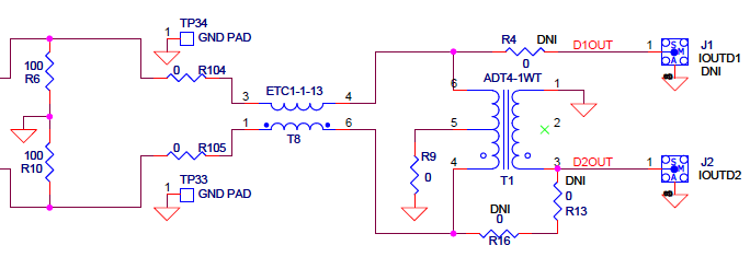
- I'm working on a sistem with xilinx Ml605, fmc-dac adapter and dac3484evm. For my experiment, I need 4 channel output. Reading the GUI dac3484evm, slac336 (it seems that doesn't exist anymore), on page 12/13 there is an optional configuration to enable the transformed coupled output. The GUI says that I need to install some resistors (short circuit). Watching the schematic in the slac481  on page 1, I see that to be able to use the outputs J2, J3, J6 and J7, I need those resitors: is that correct? And, if I place those resistors, can I use either the baseband outputs and modulated output?

- About the clock, I don't understand if I need a clock on sma J9 or if the evm can work standalone.

Moreover, my fpga has a maximum clock at 200 MHz: with this one can I get the best performances with 4 baseband channel?

- This could be a stupid question. (I apologise) Regarding the inputs on the interface J13, if I use single-ended signals, in place of differential, are there problems?

- In the end, is there any vhdl, or similar, example code? Just to understand or have an idea about the signals synchronization.

Thanks for your help.

Ciao

Simone

  • Hi Simone,

    The DAC3484 revision D and earlier had the DAC + TRF3703-15 combo. In order to use the transformer output, you will need to install R1, R3, R8, R11, R17, R161, R162, R163. You will also need to uninstall R19, R26, R27, R33, R35, R97, R98, R276. 

    Recently, we have introduced the new TRF3705 modulator with 0.25V common mode. This modulator can work with the DAC3484's output range better without the additional translation network. We have now obsolete the DAC3484 + TRF3703-15 solution due to the better solution with the TRF3705. We have also changed the DAC3484 EVM revision F to transformer output only. You do not need to change the resistor jumper option to evaluate the DAC output. The latest user's guide on the product folder page reflects this change. If you need the previous DAC EVM user's guide, please let me know and I will post it on the forum.

    To evaluate the DAC + TRF3705, you can use the TSW3085, TSW3084, TSW30H84 family of DAC RF transmitter solutions. 

    The on-board CDCE62005 can function as either a clock distribution mode or PLL synthesizer mode. For clock distribution mode, you will need to feed in an external clock to the SMA J9 connector. The PLL synthesizer mode allows the CDCE62005 to either accept the on-board 19.2MHz clock as reference or external J9 reference for the clock generator. There are some example register files in the default GUI file location of your PC that can configure the CDCE62005 in 614.4MHz, 737.28MHz, and 983.04MHz (some of the common standard clock frequencies). Other example files have the CDCE62005 configured in clock distribution mode. 

    With the FPGA output dataclk of 200MHz, this means that the maximum data rate for each channel is about 100MSPS. For 4 way interleaving input, it takes 2 input clock cycles to latch in all 4 channel data. I think the ML605 can have a faster data rate than 200MHz. You may want to double check with Xilinx on this. 

    The J13 inputs are the LVDS inputs to the DAC3484. The inputs to the DAC3484 are specified with LVDS signal level, and they have to be differential. We have some example VHDL code for the Altera platform. I will send this to you offline, and you may use this as a basis for the FPGA firmware. We currently have some discussion of the firmware in the following post:

    http://e2e.ti.com/support/data_converters/high_speed_data_converters/f/68/t/196508.aspx

    -KH

  • Very clear, perfect! Thanks of all.

    Cia

    Simone

  • Hi Kang,

    I've another question about the baseband output. I need baseband outputs with a dc offset. In particular I need signals with dinamic from 0 V to some value. Is there a way with this evm for this purpose? Otherwise, can you suggest me what could be a solution?

    Thanks in advance.

    Cia

    Simone

  • Hi Simone,

     A simple way is to set R6 and R10 to be 25 ohms each. You will need to remove T8 balun and T1 transformers to remove the AC coupling components. To route the differential pairs straight out to the J1 and J2 connector, you will need to install R4, R16, and R13 zero ohm resistors.

    With the default 20mA full-scale and 25ohm load on each leg of the diff pair, you created a 0.5Vpp SE swing (or 1Vpp diff swing) with common mode of 0.25V. This is assuming you are connecting high impedance probes to J1 and J2. If the probes that you are connecting to J1 and J2 are 50ohm, the impedance will change and you will need to adjust you R6 and R10 value.

     You may refer to the following app notes for detail. SLUA647 describes the principle of DAC3482 current source and some ways to interface the DAC with modulators. If you need to interface the DAC with amplifiers, you can refer to SLYT368.


    http://www.ti.com/lit/an/slua647/slua647.pdf

    http://www.ti.com/lit/an/slyt368/slyt368.pdf

  • ok Kang, perfect. Many thanks.

    Can I ask where I can find the schematic of the board (rev. F)? Because in the board webpage I see only the schematic file for rev. D.

    Thank you.

    Cia

    Simone

  • Hi Simone,

    The schematic is attached. We will upload the design package to the web soon.

    -KH

    DAC348XEVM-SCH_F.pdf