This thread has been locked.

If you have a related question, please click the "Ask a related question" button in the top right corner. The newly created question will be automatically linked to this question.

ADS1248 not working

Other Parts Discussed in Thread: ADS1248, MSP430F449, ADS1248EVM-PDK, ADS1118

 Sir,

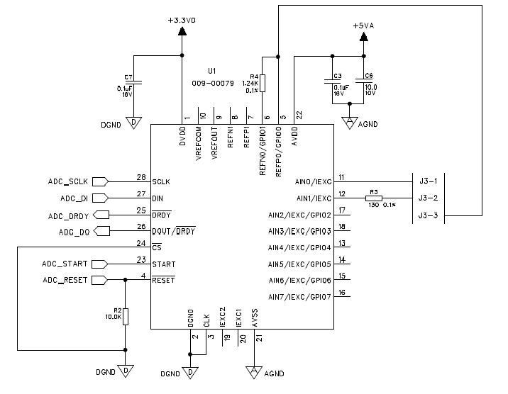
               As per our project, Three-Wire RTD Measurement using ADS1248, we need to interface pic24fj256gb106 with ads1248.As per the data sheet we programmed through SPI in the folowing manner

  • SPI1BUF=0x17;  // command to stop reading data continuously.
  • SPI1BUF = 0b01000001;       // command for writing to VBIAS reg.
  • SPI1BUF = 0b00000010;    // Command  for selectng number of bytes to be written.
  • SPI1BUF = 0b00000011;    // Data to VBIAS Reg.
  • SPI1BUF = 0b00100000;    // Data to MUX1 Reg.
  • SPI1BUF = 0b01010000;    // Data to SYS0 Reg.
  • SPI1BUF = 0b01001010;       // command for writing to IDAC0 reg
  • SPI1BUF = 0b00000001;    // Command  for selectng number of bytes to be written.
  • SPI1BUF = 0b00000110;    // Data to IDAC0.
  • SPI1BUF = 0b00000001;    // Data to IDAC1.

But we didn't get any reference voltage or digital output according to this configuration.Please suggest any solution for this problem.

Three-Wire RTD Measurement

  • Hello Gincy,

     If you could please provide an schematic to ensure we know the details of the circuit configuration, including voltage supplies, RTD sensor connections and RBIAS resistor (if used), this will be helpful.

    -  When using the  IDACs the internal reference needs to be enabled. The MUX0 settings above currently show that the internal reference is enabled and the REF0 reference input is selected for conversion.  When using the internal reference, the VREFCOM pin typically needs to be connected to GND(or AVSS) and the VREFOUT pin needs to have a bypass capacitor to VREFCOM for stability purposes in the range of 1uF-47uF.  Is the VREFCOM pin connected to GND (or AVSS)? is there a bypass capacitor between VREFOUT and VREFCOM?

    - You currently have the IDAC0 set to 1000 uA; and the VREF0 input selected for conversion.  Are you placing a resistor at the VREF0 inputs to produce the reference for conversion?

     - If you issue a RREG command, are you able to read the configuration registers without issues?

    Please provide an schematic and/or diagram showing the current circuit configuration.  Attached below is an application note that shows some examples of the ADS1248 measuring RTD's using the IDAC currents in a ratiometric configuration.

    tp://www.ti.com/sitesearch/docs/universalsearch.tsp?searchTerm=sbaa180&linkId=1

    Thank you and Best Regards,

    Luis 


  • sir,

           Thank you for your reply. As you said,i didn't connected a bypass capacitor  VREFCOM and VREFOUT. I will do that. I am not able to read the register contents by issuing the RREG command. I already placed the a resistor at the VREF0 inputs to produce the reference for conversion.i hereby attached the schematic of ADS1248 above. I expect your reply as soon as possible.

    Thank you

    Gincy

  • Hi Gincy,

    Please find a few suggestions for the schematic above:

    -  As you already have mentioned, please connect VREFCOM to AGND; and place a bypass capacitor between VREFCOM and VREFOUT; the capacitor must be in the range of 1uF to 47uF for the internal reference to be stable.

    - You have placed a 1.24kOhm an RBIAS resistor to produce the voltage reference.  Please also ensure to connect VREFN0 to AGND.

    -  The RESET pin must be held high by default; I would suggest removing the pull-down resistor R2, and instead, place a pull-up resistor on the RESET pin to the DVDD supply.

    Regarding the register settings:

    - On this circuit; the VBIAS function should not be used.  Please set the VBIAS register to 0b00000000 (disable VBIAS)

    When writting and/or reading the configuration settings, the user must held the RESET and START pins high during the communication transaction.  If you continue to have issues while writting and/or to the registers, if possible, please provide oscilloscope plots of the SPI pins (DIN, DOUT, SCL) while issuing the WREG command and another plot while issuing the RREG command.  This will allow us to verify the SPI timing.

    Thank you and Best Regards,

    Luis  


  • sir,

           As you said,i did all the changes. Before connecting VREFN0 to GND,i got a 2.5 V on J3-1 and J3-2 pins as shown in my schematic and after that i connected that pin tp ground i didn't get anything on that point and so i think I am not able to configure IDAC. I am not sure about my SPI configuration.Because when i programmed my SPI in interrupt mode, it didn't go beyond two interrupts. Is there any necessity to read back the data returned? But i can see the DIN and CLK in ADS pins and nothing is there in DOUT pin. Here   am attaching ma source code.Hope you will suggest any opinion about it.

    3618.ads.rtf

    Thank You

    Gincy

  •  \


    Sir

          Here I am attaching the graph showing the CLK and DIN in the corresponding pins by sending the SDATA command..

    Thank you

    Gincy

  • Hello Gincy,

    I did not see anything immediately wrong with the code.  The SCLK frequency appears to be set to 2 MHz and the polarity /phase appears to be correct.  However, on the oscilloscope plot above, it appears you are issuing a WAKEUP command, followed by SDATAC.

    1) When the device is powered up with START and RESET set high, the device should be by default converting at 5SPS.  The DRDY pin should show pulses showing that the conversion data is ready. In the code provided, it appears you are setting the RESET and START pin high.  Can you please confirm with an oscilloscope (or meter) that these are set high?  After powering up the ADS1248, with the START pin and RESET pin held high at default settings without writting the registers, if you place the oscilloscope probe on the DRDY pin, do you see pulses on the DRDY pin?

    2) Can you please provide an oscilloscope probe shot of DIN, DOUT, SCLK when performing the WREG communication transaction? Can you provide an oscilloscope plot while performing a RREG communication transaction?  Please confirm that RESET and START are held high and CS is held low with an external meter.

    3) After enabling the internal reference, what voltage is measured on the VREFOUT pin?

    Thank you and Best Regards,

    Luis


  • Sir,

              As you suggested, START and RESET pin held high at default settings without writing to the registers and I confirmed that the DRDY pin is showing pulses.After enabling the internal reference, I didn't get any voltage on the VREFOUT pin. Is there any problem with my SPI configuration. Can you please send me any sample codes??Hope it will help me a lot.

    Thank you

    Gincy

  • Hi Gincy,

    Attached is the ADS1248EVM-PDK firmware.  The MMB3 motherboard is based on the MSP430F449 processor. Im not sure how helpful this is going to be as we are using RTOS, and it can be rather confusing to follow.  Registers are initially written in ‘core.c’ and are changed through ‘ads.c’.  We use the built in SPI peripheral of the MSP430 and it is initialized in ‘ads.c’.  Of particular interest may be the ‘ads_reg_read()’ and ‘ads_write()’ commands that are also found in ‘ads.c’. Regarding the SPI configuration, the maximum SCLK frequency allowed is ~2.048MHz.  The Data are shifted into DIN on the falling edge of SCLK; therefore the data must be stable on falling edge of SCLK.

    6253.ads1248evm_fwsrc_1.0.8.zip


    When communicating to the device to configure the registers, I simply hold the START and RESET pins high and CS low and issue the WREG command.  In the example sequence below, the MUX1 register is configured to enable the reference; and then the MUX1 register is read:

    Device power up. Wait for supply to stabilize  (a few milliseconds)

    - Hold START/RESET High

    - Wait  ~22 milliseconds after supply is valid ( This power-on reset delay is Conservative)

    - Optional RESET pulse: Send a single RESET pulse low, ( pulse low longer than 2uS) and release RESET high.

    - Wait a Delay of ~1ms (longer than 0.6ms) after RESET pulse before starting SPI communication.

    - Issue a WREG command to configure the MUX1 register to turn on internal REF; enable onboard REF for conversion:  0x420030h.  The REFOUT pin should measure 2.048 volts after the reference is enabled.... 

    -Issue SDATAC:16h

    -Read Register MUX1: 2200XXh;

    The MUX1 register should read:x30h as expected.

    If you are able to provide oscilloscope shots of the WREG and RREG commands above of the SPI ( CS, DIN, DOUT, SCLK ) this will be helpful.

    Thank you and Best Regards,

    Luis


  • Sir,

              Thanks for your valuable suggestions. Now I am getting the reference voltage and a voltage drop of 100 mv across the sensor. So I hope that ads registers are configured properly. But I was unable to read the register values and the conversion values. when  I am trying to read ADS, it always returns a value 0x7F.What could be the problem?

    Thank You

    Gincy

  • Hello Gincy,

    - You should be able to read the register contents after issuing a SDATAC command followed by the RREG command as shown on the sequence provided above.  If you are able to provide a oscilloscope shot of the complete RREG command sequence including DIN, SCLK and DOUT this will help.

    When trying to read the conversion results, if the device is configured in the SDATAC mode, you will need to issue an RDATA command followed by 24 SCLK's. 

     If the device is configured in the RDATAC mode, the user must monitor the DRDY signal to read the conversion result.  The data can be received once from the device after the DRDY signal  goes low by sending 24 SCLKsThe user needs to ensure to complete data retrieval (conversion result or register read-back) before the next DRDY low pulse, or the resulting data will be corrupt.

    Please let me know if you are able to provide oscilloscope shots of the complete RREG sequence including SCLK, DIN and DOUT pin signals.

    Best Regards,

    Luis

  • Hello Luis.

    I am trying to meassure K type thermocouple with the ads 1247. I have the following registers values: 

    mux0=(0x08)

    Vbias=0x01

    Mux1= 0x30

    SYSO=0x40

    IDAC0= 0x80

    IDAC1= 0xff

    And when i want to read it, vbias allways shows me 0x14. 

    This is my schematic:

    I want to know if i should connect something between refp0 and refn0. Once i have the result of the conversion. Which is the equation to obtain the temperature? I am using the next one but i have no good results: 

     temperature=conversion*(2.048/16)/((2^23)-1))                 (1)

    After this i make the temperature compensation adding the respective voltage that give me the IC ds1621 and later i use the algoritm that i found in the Precision Thermocouple Measurement with the ADS1118 application note.  i suppose that Vref once i use Vbias souldn´t be in the equation (1). So my qwestion is, how should be  the equation?

    Excuse me if this qwestion is disrespectful, do you speak spanish? i´m asking you this because Bob Benjamin is helping me in another thread and my english is not so well, so there are some answers from Bob that is hard to understand to me, so if you speak spanish will be too much easy to understand to me.

    Thank you so much for your answers and sorry for my bad english.