This thread has been locked.
If you have a related question, please click the "Ask a related question" button in the top right corner. The newly created question will be automatically linked to this question.
Hi,
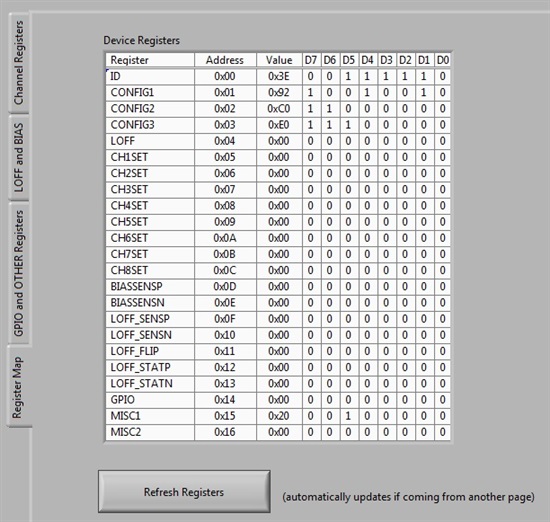
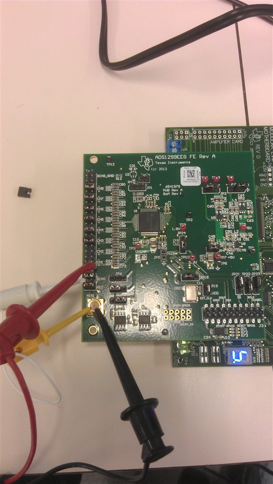
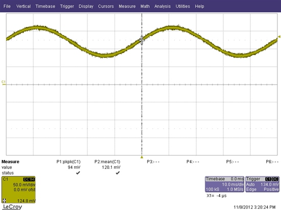
We bought an ADS1299 evaluation kit, for now i'm testing it in unipolar mode and applying an AC source to channel 1+ and Agnd with Vpeak-peak = 80mV, Voffset = 60mV, Freq = 20Hz. I set up the board as follow:
- JP2 = 2-3, JP20 = 1-2 (unipolar analog supply)
- JP7 = 2-3, JP8 = 1-2 (SRB1 to Ref_Elec)
- JP25 = 5-6, 1-2, 3 = GND
Hardware setup:
Evaluation board:
Vac source signal(goes on CH1):
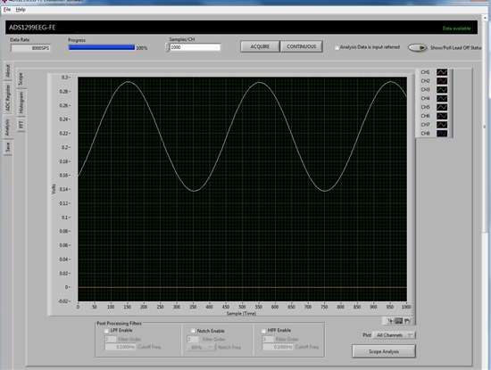
Analysis Scope gain = 1:
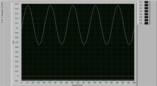
Voffset = 110mV Vpeak-peak = 80mV
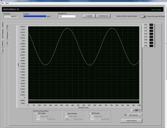
Analysis Scope gain = 24:
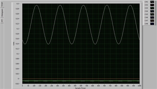
Voffset = 220mV Vpeak-peak = 150mV
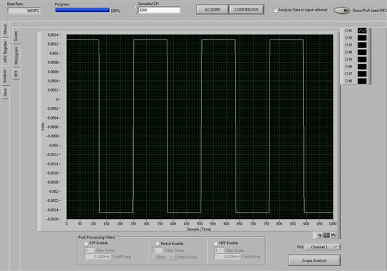
Why i dont get an amplification of 24 at graph 2? In this test i only wanted to see if the PGA works, above you can see i'm getting an amplification of max 150/80 = 1.9. Did i set up something worng? Hope someone can provide me some support with this.
thanks in advance,
Pascal -
The ADS1299 software display will by default show the data as "input referred". There should be a check box near the top right portion of the software that allows you to control how the data is displayed using this option. Further details can be found in the user guide located at http://www.ti.com/tool/ads1299eegfe-pdk
Pascal -
Are you just checking/unchecking the box after an acquisition? You will have to re-acquire the data after changing the checkbox; just changing the box doesn't not have any effect on the data.
Yes i did re-acquire after changing the checkbox. In bipolar mode the PGA works as expected, but in unipolar not. I still can' t figure out why it's not working in unipolar mode.
Could you setup a board like i did and see if you get the same results?
Pascal -
This experiment was previously performed and everything functioned as expected. Have you changed any settings from the default configuration (other than the power supply rails, JP2 and JP20?
Greg,
I have been using the default settings and routed SRB1 to gnd as reference.
I'm now using the internal test signal for debugging. In the ADS1299 datasheet following equation is given for amplitude when setting config2 bit 2 = "0" :
Vtest = 1 x (VREFP - VREFN) / 2.4mV
Unipolar supply: JP20: 1-2, JP2: 2-23
measured VREFP: 4.5V and VREFN = 0
Vtest = 4.5/2.4mV = 1875V??!
is this ment to be: 4.5*2.4mV = 10.8mV?
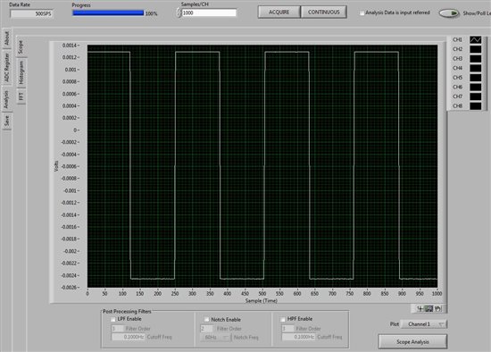
Vtest amplitude in graph: 3.7mV
Bipolar supply: JP20: 2-3, JP2: 1-2
measured VREFP: -2.3V and VREFN: -2.5V
Vtest = 0.2*2.4mV = 0.48mV
Vtest amplitude in graph: 3.7mV
The amplitude of the test signal in bipolar should be different then in unipolar, i am not seeing any difference in my graphs. Am i doing something wrong?
Pascal -
The equation from the datasheet could be the cause of your confusion. The equation should be:
1x*(VREFP-VREFN)/2.4 or 2x*(VREFP-VREFN)/2.4 with the resulting number being in units of mV (not divide by 2.4mV as it might be interpretted). Therefore for your first example, you should have something around 1.875mV.
Regarding your bipolar case, your VREF settings seem to be a little unusual. Are you really setting a VREF of 200mV (VREFP = -2.3V and VREFN = -2.5V)? If you are trying to equate your bipolar case to the unipolar case, VREFP would need to be +2.3V, and therefore +2.3V - -2.5V = +4.5V
Thanks Greg the equation was a bit confusing, but internal test seems to be working fine. I re-meseaured and in bipolar indeed VREFP = 2V and VREFN = -2V. I will report back later if i'm able to apply an external source. Thanks for you help so far!
Greg,
I have attempted another test with the board set up as described in 4.6.2 in the user manual:
1. Set all jumpers to factory defaults
2. Remove jumpers from pin 7-36 of J6.
3. Short pin 5 and 6 of JP6. Set the SRB1 bit in the MISC1 register to route the SRB1 pin to the negative input of the channels. This will route BIAS_ELEC(mid supply) tot he negative inputs of the channels through the SRB1 pin.
4. Provide the Single ended inputs to pins 36, 32, 28, 24, 20, 16, 12, 8 of J6 for channels 1-8 respectively.
Meausured voltage at srb1 pin: 2.48V, so i set my AC test source at: Uoffset: 1.24V Uamplitude: 20mV
In this case single ended inputs work: 950/40 = 23.5
So when i am using BIAS the single ended inputs work. As mentioned in my first post setting the reference electrode to Agnd instead of BIAS and routing this to all negative input channels with SRB1. I will still get the same results as in post 1: max amplification of 2. Can you explain me why this happens?
Hi,
As a side note here, from the measuring of the test signal, I conclude that the amplitude specified in the documentation is not peak to peak, but only for one phase. So the actual p-p voltage measured should be 2 * 1.875 mV = 3.75 mV for a 4.5 V reference.
-Cosmin.
According to this, the input voltage might be too high and could be saturating: http://e2e.ti.com/support/data_converters/precision_data_converters/f/73/t/354305.aspx
However, i've set the input to a constant 2.0V to IN6P. GND to IN6N. GND is same as VREFN. SRB1/SRB2 are not connected on the chip. External 4.096V reference voltage. The schematic shows how the other 4 BIAS pins are connected:
Unfortunately, the maximum gain witnessed on the ADS1299 is 1.9 (Reading is 0x79Ca16), although the gain register is set for 24x. When gain is set to 1, the reading is correct (0x3dbbcf).
I never received a response from tech support, but maybe it's an issue with way I'm initializing the other registers (Since replacing the chip did not fix the problem)?
0x0A = 0x60, Register 0x03, 0xD, 0xE and left with power-on defaults.
Any suggestions?