Other Parts Discussed in Thread: ADS1299, OPA2241, ADS1298, ADS1294R, ADS1291, ADS1198, TLC2272, OPA336
Hello,
I maybe over-read some documentation and now I'm a little bit confused in how to implement the connections between the electrodes and the ADS1299, so I'm asking here for a little guidance.
I'm using a single pole 6V power source trough 4 AA batteries, this voltage go to a TPS71202 dual channel LDO regulator configured to throw +5V and +3.3V voltages working as AVDD and DVDD respectively. I'm also using a REF5025 low noise external reference connected to AVDD and giving 2.5V, this will be used as reference voltage for the ADC in the ADS1299, this reference voltage is being divided by a basic voltage divider with two resistors and an OP-AMP buffer (OPA2241) creating the Common-Mode Voltage of 1.25V, to be used with the Bias Drive amplifier as a body reference. In short, I'm using the ADS1299 with unipolar supply and external reference of 2.5V, also the AVSS will be equal to AGND and DGND.
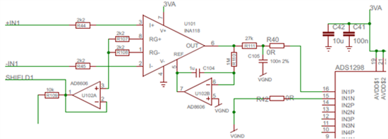
I'm developing a surface EMG acquisition device, I have look for a lot of ways of doing this interface between the electrodes and the chip, but always got confused. As first, I was following the datasheet in p.18. In single-ended input mode I assumed all the negative input electrodes will be connected to CM (Common-Mode), connecting them in-between over the body (what cares of sense for me), this confusion was developed by a schematic I found were they use a pre-stage with IN-AMPs where the two electrodes were differentiated before and then compared with CM at the same analog input of the ADS1298:
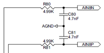
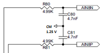
When I realized this configuration was for a unique electrode for channel then I decided to use the differential one, but all the information I have gathered for this is using (I suppose) a bipolar supply configuration, because the electrodes seems referenced to AGND by a capacitor, I couldn't be sure if is as simple as just replacing the AGND for CM. Also, I didn't quite understand why in the datasheet they talk about of a 180° phase angle between the two inputs of the channel.
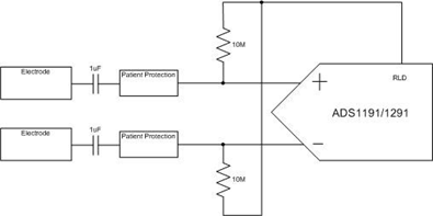
After I did an in-depth search of related topics in this same forum, the most similar case was: http://e2e.ti.com/support/data_converters/precision_data_converters/f/73/t/200221.aspx . Here the user asks for a way to correctly connect a single channel for ADS1298. He got as answer the diagram showed later; there is no connection to AGND or CM between the two electrodes, but a connection to RLD_Out through a high impedance resistor. This got me a lot more confused. Then there is no necessity to connect a CM? This configuration just work for one channel or could be configured to multiple ones?
So, my questions for the community are:
- How could I correctly interface the electrodes to the ADS1299 taking into account that I’m using a unipolar supply and an external ADC reference?
- How should be configured the Bias Drive channels internally (of the ADS1299) to work with multiple inputs? I'm talking about MUXx[2:0] and BIAS_SENSx[x] registers.
- Should I use the internal Bias Drive amplifier as a buffer for another amplifier or it’s enough if I put the filter there?
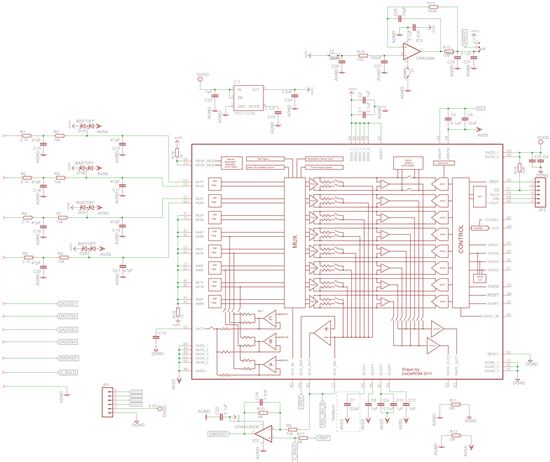
- I’m only taking into account a Bias Drive Electrode, but in the user guide for the ADS1299EEG-FE there is a Reference Electrode, what’s the differences between those? Do I need both?
- In other users configurations as in the same user guide mentioned earlier I have seen a “shield” connection with the Bias Drive Amplifier (or RLD also), where is this pin connected to? Is this necessary?
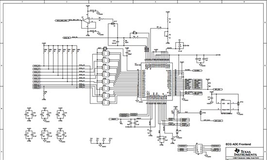
- Lastly, at the ADS1298 FAQ section of this forum says that unused pins should be connected to AVDD, and I actually could see that implemented in the schematics of the ADS1298ECG-FE, but not in the ADS1299EEG-FE schematics, is this AVDD connection necessary for ADS1299?
I hope this could be helpful for other users, not just me. Also I have taken a lot of assumptions; I would appreciate if with the answer you correct me of undetected misconfigurations I already have supposed.
Thanks in every way!


