Because of the holidays, TI E2E™ design support forum responses will be delayed from Dec. 25 through Jan. 2. Thank you for your patience.

This thread has been locked.

If you have a related question, please click the "Ask a related question" button in the top right corner. The newly created question will be automatically linked to this question.

ADS1256 strange problems

Other Parts Discussed in Thread: ADS1256, UC3854, ADS1252, OPA4350, OPA2350, OPA350, ADS8515, ADS8517, ADS8555, OPA211, NE5532, ADS1282, ADS1248, ADS1259, ADS131E08, ADS1271, REF5025, ADS1258, PGA117

hi 

its since now almost 47th day struggling with ads1256 ic to run this beast but still not able to run this ic

i have constructed prototype pcb to test functionality of ads1256 ic

at first there was no output on serial data out pin of ic at that moment i used 3.3 volt from microcontroller power supply but there was no sine of any data even no signal on ads1256 drdy pin then i had to add dedicated 3.3 volt regulator to ads1256 dvdd power pin then it start showing signal on drdy pin after that since now i am facing strange behaviour of ic 

i tried to change output values on digital io pin and it works with out any problem it changes output value i have attached a led to see the result 

whenever i try to adjust data rate register ads1256 drdy pin shows strange signaling even 1 to 2 second long switching signal on this pin where high and low signal have no correlation that it will be same pattern for all time

then i issue data rate adjust command continuously  to set data rate value register it still did not works until i remove power from ads1256 ic and until it starts with default data rate setting and then with multiple issue of data rate adjust command it shows drdy signal as expected  

at this point i have these question 

why it does not work with common digital power supply rail where many other digital pheripharal work normal and even power supply ripple is less then 20 mv in worse case on its digital power rail

why it requires individual voltage regulator 

why it didn't accept command on the first time issue of the command 

how many times commands should be issued so it will perform required function specially data rate adjust procedure

there is no timing digram for data rate adjust command in data sheet and command sequence so what is correct sequence of this command 

what is the allowable maximum spi clock frequency @7.2 mhz and @10mhz of crystal oscillator 

how to calculate data rate on different clock frequency of adc

we are willing to use this adc in programmable power supply project but this beast is still not functioning properly

hope to get quick reply

regrads

Shams iqbal 

  • Hi Shams,

    Welcome to the TI E2E Forums!

    Regarding your questions:

    shams iqbal1 said:
    why it does not work with common digital power supply rail where many other digital pheripharal work normal and even power supply ripple is less then 20 mv in worse case on its digital power rail

    The ADS1256 requires two power supplies: A 5V analog supply (AVDD) and a 1.8V to 3.6V digital supply (DVDD). Both AGND and DGND should be connected together so that the supplies are at the same potential. The ADS1256 will pull approximately 1mA of current from the digital supply in normal operation. Assuming your digital supply is capable of powering all your peripherals, there should be no problem.

    shams iqbal1 said:
    why it requires individual voltage regulator 

    The ADS1256 does not require it's own voltage regulator. I do however recommend providing individual decoupling capacitors near the AVDD and DVDD pins.

    shams iqbal1 said:

    why it didn't accept command on the first time issue of the command 

    how many times commands should be issued so it will perform required function specially data rate adjust procedure

    Commands only need to be issued once. Assuming the device is powered and it's getting the master clock from from an external source like a crystal oscillator, check the SPI signals to make sure they are correct. I'll check your SPI sequence and timing if you provide an oscilloscope screenshot of the SPI communication. It's also worth checking your oscillator to make sure it is starting properly.

    shams iqbal1 said:
    there is no timing digram for data rate adjust command in data sheet and command sequence so what is correct sequence of this command

    I recommend beginning all SPI communication with the SDATAC command. Then issue the two commands bytes for WREG (for example: 0x53, 0x00), followed by the data byte (0xA1 for 1 kSPS).

    shams iqbal1 said:
    what is the allowable maximum spi clock frequency @7.2 mhz and @10mhz of crystal oscillator 

    The t1 timing requirement (SCLK period) on page 6 says the maximum SCLK frequency is 1/4 the master clock/crystal oscillator frequency, so 1.8 MHz and 2.5 MHz, respectively.

    shams iqbal1 said:
    how to calculate data rate on different clock frequency of adc

    The data rates in the data sheet assume you are using the nominal 7.86 MHz master clock. As you scale the master clock the data rates will change proportionally. If you use a 10 MHz master clock and set the data rate to the 1kSPS setting, you will actually be running at:

    (10MHz / 7.68MHz) * 1 kSPS =  1.302083 * 1 kSPS = 1.302083 kSPS.

    I hope my responses help. I'd also be happy to review schematic if you are willing to share.

    Best Regards,
    Chris

  • dear thank you for clearing me about my question 

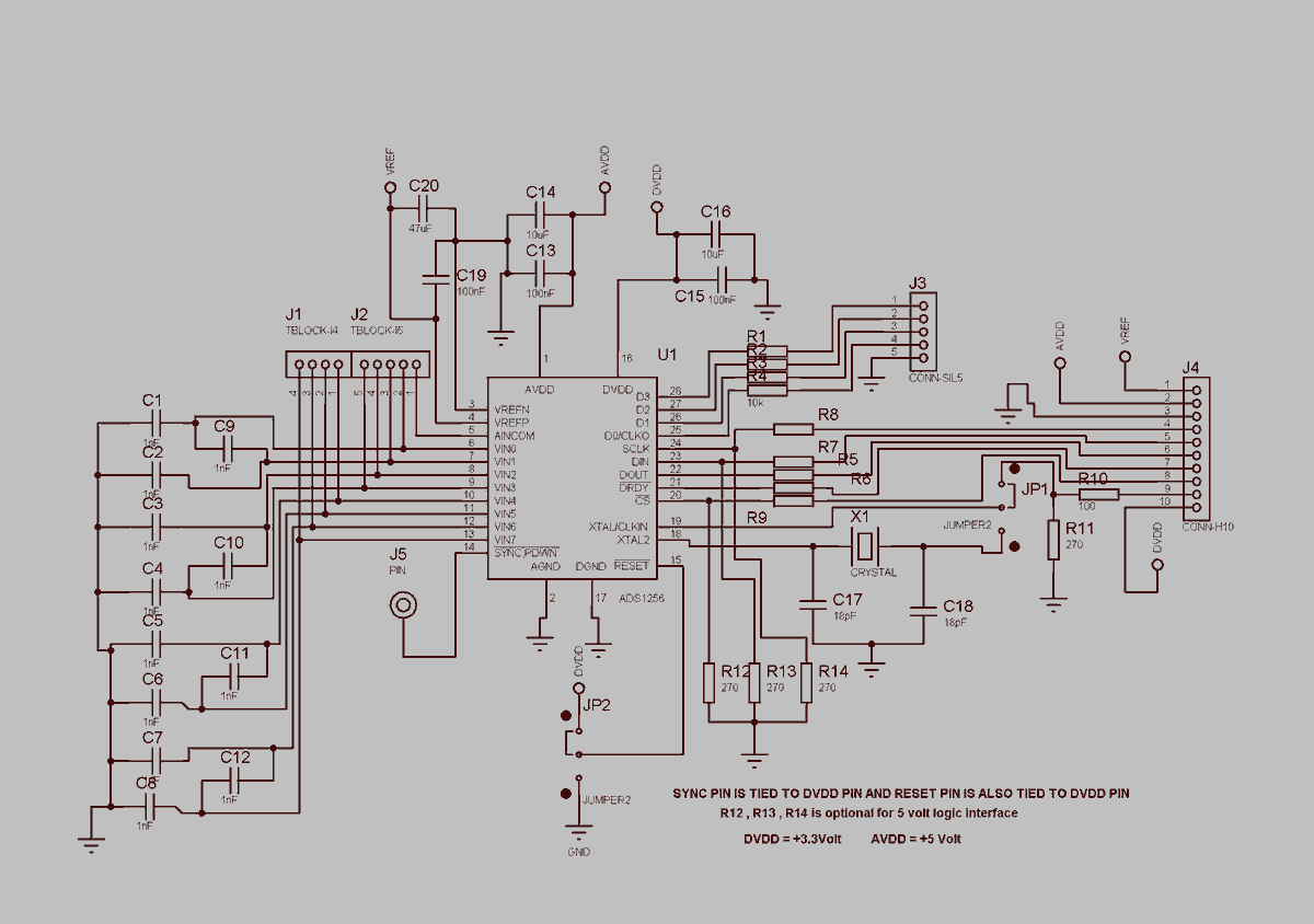
    here is prototyping digram and layout which i am using 

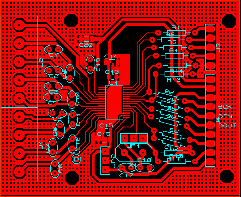
    and here is layout 

         NOTE: here i will mention that this is just for ads1256 functional testing purpose prototype 

    i had already connected tantalum capacitor to ads1256 dvdd power pin using le33 (3.3)voltage regulator and same power rail was spouse to provide power to atxmega64a4u microcontroller  placed on bread board  there was no sign of any data on ads1256 dout pin i had used oscillator module to provide clock to ads1256 and i was able to confirm that ads1256 ic is running by watching clock signal on clko/dio0 pin while reset pin and power down pins are shorted together with dvdd pin even no drdy signal output at that time

    then i moved to stm32vl discovery kit to check the problem but result was same no luck at all unless i have added individual le33 voltage regulator on ads1256 dvdd power rail and nothign else is connected with it and then suddenly it showed up drdy signal output

    after that i attached crystal to to use internal oscillator of ads1256 ic and it started well with out any problem and for oscillator starting monitoring purpose i have added a led to clko/dio0 pin along with 470 ohm resister in series of led to check if any time internal oscillator is hanged or not 

    for voltage reference i have constructed a saprate PCB which is working properly  and clean 2.5 volt using recommended buffer drive ic in data sheet of ads1256 ic 

    now back to command set 

    after power i use interrupt based sequence to detect drdy signal of ads1256 then i shift out command Sdatac = &H0F after that i shift out  command Wreg = &H53 and &H00 along with valid drate value now this seems to work ok i can see the drdy signal timing is changing according to data rate adjustment 

    but after that if i try to read adc result it did not shows any values right now i am working on ads1256 note these ic are sample ic's which i get directly from TI sample centre and i am not sure that these ic are working like the one available for purchase or not same functional

                             this not the first time i got stuck with TI ic's i will mentioned that the an other ic uc3854 (the data sheet is still not corrected) when i waisted allot of time and result was zero and sadly i chosen fairchild ic for that project and that worked at first time without any problem 

    now you are mentioning that every command must be issued by using sdatac command well that gives some response plz add this line in data sheet of ads1256 

    i don't know who wrote the data sheet of this ads1256 ic who just saved words to not to described functional behaviour of ic specially starting condition and first command that must be issued to this beast so it will give some response well i am still trying and i will update scope capture data in after few more tries 

    regards 

    shams iqbal

  • Hi Shams,

    Are you populating R12, R13 and R14? I assume the logic levels are compatible and those are unnecessary.

    Since you're using multiple boards, are you being careful to connect the grounds of all PCBs? It's a simple thing that gets overlooked quite often.

    Is there a bottom layer on your prototype board? There should be a ground plane below your SPI (and power) traces. Without it, you're trying send very fast signals through inductive traces. Your digital signals may be very distorted when they reach the ADS1256. (The power traces are also going to be highly inductive without a ground plane beneath them. Even though they are thicker, the return current has to travel a big loop area which is shared will all of the digital return currents.)

    shams iqbal1 said:
    but after that if i try to read adc result it did not shows any values right now

    What is your command sequence for reading data and are you delaying between commands to meet the t11 time requirement? The ADS1256 acts like a state machine. The timing requirements provide time for the state machine to decode the command sequence and change states before it receives the next command. Here's an example of writing to the registers, restarting the ADC conversion, and reading data:

    ads1256_cmd(ADS1256_SDATAC, 0);			//SDATAC Command
    
    ads1256_wreg(ADS1256_ADCON, 0x20);		//WREG ADCON - default, PGA = 1
    __delay_cycles(6*4);				//DELAY
    ads1256_wreg(ADS1256_MUX, 0x01);		//WREG MUX - CHANNELS AIN0-AIN1
    __delay_cycles(6*4);				//DELAY
    						//t11 delay (4*tCLKIN) after WREG command 
    						//MSP430 CLK is ~6x faster than ADC CLK
    
    ads1256_cmd(ADS1256_SYNC, 0);			//SYNC
    __delay_cycles(6*24);				//DELAY
    						//t11 delay (24*tCLKIN) after SYNC command 
    ads1256_cmd(ADS1256_WAKEUP, 0);			//WAKEUP
    
    ch32_code = ads1256_drdy();			//FXN that reads 3 bytes
    __delay_cycles(6*4);				//DELAY
    						//t11 delay (4*tCLKIN) after RREG command 

    shams iqbal1 said:
    these ic are sample ic's which i get directly from TI sample centre and i am not sure that these ic are working like the one available for purchase or not same functional

    Our sampled parts are exactly the same as purchased products.

    shams iqbal1 said:
    now you are mentioning that every command must be issued by using sdatac command well that gives some response plz add this line in data sheet of ads1256

    You only need to send SDATAC once to exit the "read data continuous" mode. You would then only need to send "SDATAC" again at some later time if you sent RDATAC to enter back into the "read data continuous" mode.

    Best Regards,
    Chris

  • hi 

    thank you for your help dear as i mentioned in diagram that R12, R13 and R14 are optional because at starting i faced problems with 5 volt logic interface but now its working ok and cs pin tied to ground permanently 

    here i want to confirm one thing that  if my command took longer time then single drdy cycle then what would be response of ads1256 just like 

    ads1256_cmd(ADS1256_SDATAC, 0);			//SDATAC Command

    specially when my spi interface clock is slow speed and how slow spi clock can applied when ads1256 running on 7.2 mhz crystal

           what is role of drdy signal does all command should be synced with drdy signal or we can issue commands(except conversion data read) at any time specially when

         cs pin of ads1256 is permanently tied to ground

    or

         cs pin is controlled by software 

          is there any valid role of cs pin between each command just like if we use serial sram from microchip its necessary to use cs pin for mostly commands to terminate effect of previous command and to issue new command   

           if i use cs pin then what if cs bring high during middle of write register command      like hardware cs control between every byte transmit and some delay to move second byte to spi transmit buffer this things cause spi cs pin to high  in middle of each three byte transfer from mcu to ads1256 

         or we have to use cs pin using software control 

    i have some TI DSP mcu's though but tools for debugging and programming are little costly and i am looking for some ecnomical debugging tool while St microelectronics made it possible to get nice prototyping tools with on board debugger on board mem's sensors with audio codec ic

    only at the price of 14.9$

    while other COLOUR TFT LCD PROTOTYPING board is available only 22$ price that one is also the cheapest board available in the market with tft lcd on board including on board debugger from ST microelectronics

    sorry to go for off topic but i am mentioning this thing here because every time when you go to design a new product its very hard to invest allot of money on development tools specially when your product is dedicated with very low quantity and sell price of that product even not higher that makes difficult to stay on only one brand 

    well about different hardware so about me i am designing products since 1998 and this design will be finalized on atxmega64a4u microcontroller which is 3,3 volt working part due to ads1256 dvdd working limit i switched different hardware because i want to make sure that i am not doing any thing wrong then i checked oscilloscope wave forms to again verify that i am doing right before asking on post and its not me my two application engineers was not able to run this ic until i personally get involved in this project and i hope so that after this i do not feel any need to ask further help relating to  8 channel 16-bit dac ic also from ti  which will be used in the same project 

    here how it happens in ads1256 on power up until if we did not issue the sdatac command it does not gives you proper response to further commands plz correct me if i am wrong at this point and now i am confirmed that data on ads1256 is latched on falling edge of spi clock while spi dout line idle low state 

    how we want to use this adc ic i am going to mention

    we want to read eight analog channels at 50hz sampling rate where four channels will be read using gain stage with ain common pin for common inputs to all eight channels so what would be valid code for this type of function with valid timing delays between each command for each conversion and what will be role of drdy pin with each command plz share timing digram waveforms of each command so it would be easy for me to understand 

    regards

    shams iqbal

  • Hi Shams,

    shams iqbal1 said:

    here i want to confirm one thing that  if my command took longer time then single drdy cycle then what would be response of ads1256 just like 

    ads1256_cmd(ADS1256_SDATAC, 0);			//SDATAC Command

    specially when my spi interface clock is slow speed and how slow spi clock can applied when ads1256 running on 7.2 mhz crystal

    First, here is what a SDATAC command should look like on the SPI bus. Note that /DRDY is low while the command is issued.

    The SCLK must be at least 10x the speed of the data rate, however, it is easier to meet the timing requirements with a faster SCLK closer to 100x the data rate.

    With a 7.2 MHz crystal, SCLK must be less than (7.2 MHz / 4) = 1.8 MHz.

    shams iqbal1 said:

    what is role of drdy signal does all command should be synced with drdy signal or we can issue commands(except conversion data read) at any time specially when

         cs pin of ads1256 is permanently tied to ground

    or

         cs pin is controlled by software 

    It is an oddity with the ADS1256 that some commands must be synchronized with the state of /DRDY. It has to do with the way the digital state machine was implemented. As such, certain commands are only expected to be issued after a conversion completes (when /DRDY goes low).

    Permanently tying /CS to ground is okay. However, if you have a GPIO available for it, I recommend using it. If SPI communication were to get out-of-sync with your micro (for example if there was a clock glitch), toggling /CS would allow communication to recover.

    shams iqbal1 said:

          is there any valid role of cs pin between each command just like if we use serial sram from microchip its necessary to use cs pin for mostly commands to terminate effect of previous command and to issue new command   

           if i use cs pin then what if cs bring high during middle of write register command      like hardware cs control between every byte transmit and some delay to move second byte to spi transmit buffer this things cause spi cs pin to high  in middle of each three byte transfer from mcu to ads1256 

         or we have to use cs pin using software control 

    /CS is not needed to terminate and issue new commands. It is primarily there to allow sharing of the SPI bus with other SPI devices. If /CS is HIGH, the ADS1256 ignores any commands on the SPI bus.

    /CS should be held low for the full-duration of the serial communication. If you interrupt a "write register" command before it completes, it will not update the register. You'll have to re-send the complete write register command again.

    shams iqbal1 said:
    i have some TI DSP mcu's though but tools for debugging and programming are little costly and i am looking for some ecnomical debugging tool

    Our microcontroller groups have been making a lot of developments on low-cost evaluation modules. If you haven't heard of our LaunchPad platform, I recommend checking it out here: http://www.ti.com/launchpad.

    shams iqbal1 said:
    now i am confirmed that data on ads1256 is latched on falling edge of spi clock while spi dout line idle low state 

    DOUT may not always idle LOW; I've seen it idle HIGH too. You're correct about data latching on the falling edge. The SPI mode is CPOL=0; CPHA=1.

    shams iqbal1 said:
    we want to read eight analog channels at 50hz sampling rate where four channels will be read using gain stage with ain common pin for common inputs to all eight channels so what would be valid code for this type of function with valid timing delays between each command for each conversion and what will be role of drdy pin with each command plz share timing digram waveforms of each command so it would be easy for me to understand 

    Similarly to the code above: Issue SDATAC, then issues all of the WREG commands to configure the ADS1256. Then you would cycle through channels as shown in figure 19 in the data sheet:

    The important delays to pay attention to are t6 and t11. They are delays between bytes as shown in figure 1, page 6 in the data sheet:

    The table on the same page lists all of the commands that require these delays.

    Best Regards,
    Chris

  • dear 

    thank you very much for your help 

    at this point i learned that there was some missing key point to use this ic and those was 

    1) after power up of ads1256 sdatac command must be issued so it will accept any further command 

    2) every command should be issued by syncing drdy signal to get proper response from ads1256 ic

    3) t6 and t11 must be added with respect to what type of command is issued

    4) cs is not necessary but beneficial for some point of operation to terminate unfinished command 

    5) provide individual voltage regulator for ads1256 dvdd power supply because it did not start properly many times and it is confirmed on other posts also that it is little more sensitive to emi /esd noise so provide maximum isolation from any kind noise to its dvdd pin line and tvs diode is must on its dvdd pin 

    finely we had managed to run this ic with your informative help and we are very thank full for your guidance 

    well at this point i have analysed that this adc is good candidate for precision measurements but its state machine is real problem and on the other hand this ic is sensitive to esd/emi noise 

    and if we go for 2.5 hz update rate then we can get 20bit resolution which is noise free but above then  only on 10hz sample rate its noise free bits reduced to 17-bits 

    any how this our economy class product but for really high precision we are still looking for better replacement part which works more robust in esd/emi noise and provides 20-bit accuracy for all 8 channels and at-least 5 samples/Sec per channel so plz suggest a suitable product or solution for this requirement where we want to use 20-bit dac for analog control signal i am going to mark this post answered as now this project is again going to hand over to our application engineer for further development where it will be finalized on minimum of four layer PCB to gain maximum performance 

    now dear i have another adc in list for another project and that's part no is ads1252 here we have some confusion relating to its operation plz guide us for its interfacing my question is what is the reset state of drdy/dout pin function

    just like

    if i pulled high serial clock line  for five drdy cycles and released serial clock line to low then what should i consider to that what is the current drdy/dout function status and how to calculate adc clocks for one drdy cycle basically i want to use timer counter to determine dout status for data reading and once it is synced with timer so i can easily read the data from it  while adc clock is being supplied from micro-controller so clock syncing procedure will work with out any problem and free up the processor for other tasks

    regards

    Shams Iqbal

  • Hi Shams,

    Regarding your comment on noise performance:

    shams iqbal1 said:
    and if we go for 2.5 hz update rate then we can get 20bit resolution which is noise free but above then  only on 10hz sample rate its noise free bits reduced to 17-bits 

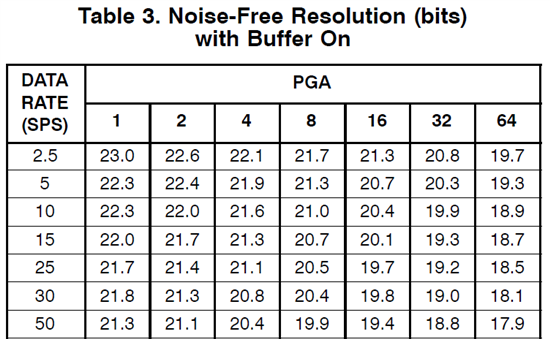
    The ADS1256 should be giving you 20 bits noise-free resolution at 10 SPS. Table 3 tells you the possible noise-free performance (measured with shorted inputs). In most applications there will be some noise degradation because we don't care to measure shorts, but real signals which have noise.

    Note that the noise-free resolution goes down with the PGA gain. However, for each binary increment of gain, the signal amplitude is doubling and the noise-free resolution decreases by less than 1 bit (Noise increases, but not as much as the signal amplitude). Therefore, you are actually gaining resolution as the PGA gain increases.

    Regarding your question on the ADS1252:

    shams iqbal1 said:
    if i pulled high serial clock line  for five drdy cycles and released serial clock line to low then what should i consider to that what is the current drdy/dout function status and how to calculate adc clocks for one drdy cycle basically i want to use timer counter to determine dout status for data reading and once it is synced with timer so i can easily read the data from it  while adc clock is being supplied from micro-controller so clock syncing procedure will work with out any problem and free up the processor for other tasks

    Holding SCLK high for 5 clock cycles resets the modulator, which is what you're trying to do. The reset happens about on the falling edge of SCLK. Actually, reset will be on the first falling edge of CLK after the falling edge of SCLK. So unless your SCLK is derived from the CLK, you'll know within one CLK period when the reset happens.

    A time "t14" after reset occurs (t14 = 2042.5 * CLK) is when the first /DRDY pulse occurs. However, data is not valid until the 6th /DRDY pulse because this is not a single-cycle settling device like the ADS1256. Therefore, you'll need to wait an additional five t_DRDY time periods. So your first timer will start on the falling edge of SCLK, and count down from (2042.5 + 1 + 5*384) * CLK or 3,963.5 CLK periods. Then every following timer needs only to count 5 (or 6) t_DRDY time periods or about 1920 (or 2,304) CLK periods.

    Best Regards,
    Chris

  • dear 

    thank you for your reply as you mentioned for ads1256  relating to graph i did not find it like that 

    how we can see the noise free bit simply shorting the two input pins of adc which is select for analog reading 

    but what i had seen that on 2.5 sample/sec 20bits are noise free and last four bits are changing randomly just changing sample rate to 10 is shows 17-bit noise free and remaining 7-bit shows random noise for Vref i used ref5025id high grade ic with opa4350 as buffer amplifier actually i developed ads1252 evolution set-up to se that what i can get from that one but result was even very poor i used same application circuit which was shown in ads1252 data sheet for +/-10 volt reading instead of opa2350 i used opa4350 quad version of opa350 and i used two opamp for ads1252 one for buffered ref out put  with heavily filtering capacitors i placed 22uf capacitor on ads1256 pcb very close to ref pin and total capicotor value is not more than 60uf but no result as i was expecting from ads1256 .

    any how i figured out that delta sigma is bad choice for high precision measurements very tough to drive and very difficult to stuff on pcb even noise issue is a big problem and pcb requirement is minimum four layers which is not suitable for economical design if i calculate price that would be more than 100$ for control board including two 16 bit dac for single channel power supply so at this point plz guide me what will be better choice to make it more economical any other high precision adc and dac you recommend for my product here are the things which i need

    6 digit volt meter and current reading (1,2 or 3 channel for volt and 1,2 or 3 channel for current )

     16-bit dac for volt and current set point (2 dac for single out , 4 dac for dual out and 6dac for tripple out put version)

    any better power stage control circuit in single ic package form or with minimum ic's count to control power transistor(npn ,pnp,mosfet) for volt and limit current  with 0 to 60 volt and 0 to 6 amp setpoints where we can adjust 1 millivolt set point for volt (60000 count of dac )and 0.1 milliampere current limit set point (60000 count of dac )where our read back scale using adc will be  0.1 millivolt for volt and 0,01 milliampere for current and adc sample rate should be at least 12 samples/sec to see the output on display effectively 

                        i have already worked on control stage in linear voltage regulator mode with npn transistor but still looking for better choice any of your guide relating to component choice and circuit design will appreciated which will result to make it more economical due to delay on production target date now we are also focusing to look analog devices or linear technology  components to make it more economical

    regards

    Shams Iqbal 

  • Hi Shams,

    Delta-sigma ADC's are widely used for high-precision measurements. No other type of ADC provides as much resolution. SAR ADCs will have the next highest resolution, but they also require good driving circuitry. SAR ADCs usually require higher bandwidth drivers than delta-sigma ADCs, and it is harder to find SAR ADCs with integrated drivers.

    Designing precision data acquisition systems with 24-bit delta-sigma ADCs is challenging because you're able to measure signals in the nano-volt range! Even with the best ADC, it requires high quality components, voltage reference, and PCB layout to reduce the overall system noise. 4-layer PCBs are probably the most common. It is possible to do 1- and 2-layer PCBs with these applications, but it is very challenging!! 4-layer PCBs have become cheaper and they will probably save you on the overall PCB area.

    You mentioned your application:

    shams iqbal1 said:
    6 digit volt meter and current reading (1,2 or 3 channel for volt and 1,2 or 3 channel for current )

    Let me know what level of resolution, sampling rate, and input signal voltages you're trying to measure and I can help direct you.

    As far as the DAC and power management blocks, those are not my area of specialty. I'd recommend asking a question in the E2E Power Management forum. For the DAC, it's best to start a new thread in this forum.

    Regards,
    Chris


  • dear 

    i am glad that i got very good response from TI and their application engineer and i will be very thankful for you about further help regarding to my application  i will request that redirect some one from power and dac relating application engineer who will give me better way about components choice and their  application either here on community or on my email address 

                     at this point  lets start the designing process my maximum voltage reading will be 100.0000 volt dc and 10.00000 amperes dc i mentioned digits to show the scale factor where two channel will shows 100.0000 volts dc range (one for positive and one for negative volts with 100u volt precision)and one will shows 10.000000 positive dc volt (10u volt precision) three channel will shows 10.00000  ampere dc  (two positive dc amperes and one negative dc amperes @ 10u ampere precision) range while per channel sample rate should be minimum 2sample/sec so total 12 samples/sec and preferred is 4 (samples/sec)/channel and total gross 24 samples/sec

    where channel means volt or ampere reading input 

                         we have our own pcb manufacturing   but only for single and double layer pcb's mostly time we prefer single layer pcb for quick production and cost reduction purpose while double sided pcb consume more time and cost is high so my prefer target is 1)single sided pcb or 2)single side routing with other side  layer of ground plane and at last is 3) full double sided pcb  so  guide me as per described basis that what is best pcb layout to get target performance

              currently i have these components available in my inventory list and i will be glad if you help me out to find better and economical components relating to my application if email support is faster then plz proceed via email so this is my inventory list

    PART NO DIGIKEY PRICE
    ADS8517IBDW 36.9
    ADS8555SPM 26.91
    ADS1282IPW 63.34
    ADS1248IPW 11.76
    ADS1259BIPW 15.74
    ADS8515IDB 23.31
    ADS131E081IPAGR 12.16
    ADS1252U 15.35
    ADS1271B 18.02
    ADS1256IDB 14.91

    now you can see the manufacturing cost is the major issue 

    ads8517 /ads8515 built in ref and ref driver circuitry easy input drive can be used with analog multiplexer and over sampling with dither method will give high resolution even with high sample rate then delta sigma adc i also posted about this thing in this link but did not get any attention from any one 

    http://e2e.ti.com/support/data_converters/precision_data_converters/f/73/t/310318.aspx

    ads8555 built in ref and 6 sar adc in a single package but requires input driver for each adc channel same thing oversampling for high resolution and nearest driver for input is ne5532 with compare to opa211 / opa2211 and very price competitive little loss of performance can be gained from oversampling if using ne5532 for driver stage 

    ads1282 very costly but have good specifications 

     ads1248 every thing is best

    Low-Noise PGA: 48nV at PGA = 128 4

    Differential/7 Single-Ended Inputs 

    Very Low Drift Internal Voltage Reference 

    Analog Supply Unipolar (+2.7V to+5.25V)/Bipolar (±2.5V) Operation

    Internal Temperature Sensor which is usable to determine voltage ref temp drift error for compensation 

    Self and System Calibration

    Single-Cycle Settling for All Data Rates

    Simultaneous 50/60Hz Rejection at 20SPS

    and price is also very economical but ohhh noooo input impedance that's very wrong 400 ohm only what to do about that input impedance

    ads1259 have good specifications but single channel and requires input driver and multiplexer for reading six channels which increase cost and complexity but if economical driver stage and multiplexer option is available then its far best due to its data sheet specifications

    ads131e08/06 for eight /six channel Analog Front-End but did not got chance to test the performance and price is also very good can you plz give me review about this part that what maximum output performance can be achieved using this ic by extra oversampling like using 1k sample/sec and further oversampling down to 4 or 2 sample/sec in external micro-controller

    ads1252 very difficult to interface no voltage reference and no input stage driver poor performance high cost

    ads1271 high sample rate but i have seen 17 bit performance with normal buffer opamp driver on bread board and i belive that oversampling will give the required performance but again cost is issue

    ads1256 this is good ic but tough to drive in my past experience single channel 20-bit result on prototyping with application circuit described for voltage ref in datasheet and input shorted settling time is another issue voltage reference and buffer itself is very costly causes to increase the manufacturing cost but here i will ask one more question about that what is the purpose of opa350 buffer for ref input stage while if i use ref5025 ic it can provide sufficient drive current and according to data sheet ref input impedance of ads1256 is 18.5k ohm so plz provide some detail about this that what be result if i directly connect ref5025 ic output to ads1256 vrefp pin and if buffer is necessary then what alternative circuit can be used with more common parts which are less costly 

    now this is my servey about TI adc ic's price feature performance description and distributor price may be i left some things far more better and economical components from TI that's why i am here to get help from application specialist hoping for better guide from TI application engineer

    regards

    Shams Iqbal

  • Hi Shams,

    So you need about 20-bit noise performance and 6 channels (3 for voltage measurements and 3 for current measurements and positive & negative signals are on separate channels). Do you need to simultaneously sample any of the channels or can you multiplex between all 6 channels?

    How do you plan to implement the analog front-ends? Will you use resistor dividers to match the input voltage range to the ADC's input range?

    Do you need to isolate between channels? If, so you may need to use voltage and current transformers, otherwise use multiple single-channel ADC's.


    The higher speed ADC's will most likely not meet your noise performance requirement. Also due to the number of (multiplexed, non-isolated) channels and the need for input buffers, I would direct you towards the ADS1248, ADS1256 or ADS1258.

    • The input impedance of the ADS1248 is much higher than 400 Ohms. You're looking at the output impedance of the bias voltage, which is only needed for a floating sensor input like a thermocouple.

    • Using an OPA350 to drive the ADS1256 reference input is probably overkill. You would most likely be okay using the REF5025 to drive the ADS1256 directly.

    Regards,
    Chris

  • dear 

    thank you for your reply 

    well there is no need for simultaneous update rate for all channels and for input stage  i will use  buffer amp for each volt/current reading because

    for positive 0 to 100 volt reading  dc potential can be applied directly to adc input after scaling due common ground but for negative volt 0 to -100 volts i will use inverting buffer amplifier (note i will use split/complementary supply for adc buffer amplifier) all amplifier will be used in four gain setting option using relay/74hc4052  switch for fine volt /current reading here i have one more question from you if i use 74hc4052 for gain selection then what would be the overall impact on required performance 

    well i had seen data sheet for ads1258 and Table 6. Noise Performance  18.9 noise free bit which is less then 20 bit noise free resolution so how to deal with this ads1256 have good performance  i am considering to use ref5025id ic for vref of ads1256 where i can add 47uf capacitive load on ref5025 output can you plz verify the performance in this way on ads1256evm by bypassing buffer amplifier opa211 and using ref5025id with 47uf capacitor on vref output directly connected to ads1256 vref pin so i will be confident about my circuit and what would be long-term drift error in case of this heavy capacitive load on ref5025id out put

    well about ads1248 that is economical version so what would be proper circuit for this adc would you recommend this adc for my required performance 

    at the moment i have these two parts available in my hand ads1256 and ads1248 and for ads1258 i have to wait until i recive ads1258 adc ic 

    i am curious that you did briefed on ads131 is this not suitable for my application while i need only 4 samples per channels and after internal over sampling only 1k sample/sec is available where i have enough computing resources available in micro-controller to further oversampled 256 times adc result to get more noise free bits 

           i have also pga117 in my stock(which we already using in data logger products) and according to data sheet ads1259 can provide 16 samples/sec at 21 noise free bit resolution   i exactly need scope gain for volt current display and pga117 have scope gains where pga117 will cost 4.8$ +ads1259 will cost 15.74$ and that will be total  20.54 $ and thats more economical but how to fit these two ic's together for 20bit performance now if you help me out to solve this chicken and egg mystery i will be very grateful to you

    for current measurement single low side current sense amplifier will be used 

    for third channel i will use isolation amplifier and in any case if i am not able to get six channel measurement at 20 noise free bits from single adc ic then i will use additional adc for third volt/current channel 

    regard 

    Shams Iqbal