This thread has been locked.

If you have a related question, please click the "Ask a related question" button in the top right corner. The newly created question will be automatically linked to this question.

ADS7825 Internal operation

Other Parts Discussed in Thread: ADS7825

Hello,

There is something that I want to confirm about the operation of the ADS7825.

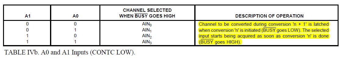
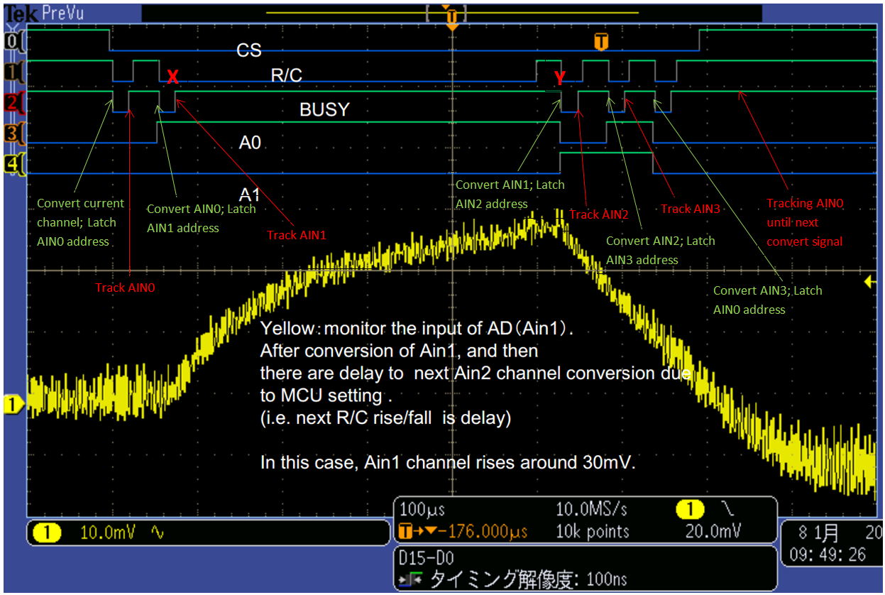
Q1.What is the reset voltage level of sampling capacitor before a new sample is taken?

Q2.Which is the position of the sampling switch immediately after conversion complete open and closed?(when BUSY goes logic high)

Best regards,

Seishin

  • Hi Seishin,

    Before I proceed I'd like to know if there is a specific issue you are facing with the ADS7825 that has prompted your questions (esp. your first question). Please note that this part is over 20 years old and getting information on specific design details may take some time. I will discuss your first question with the Design team next week and get back to you.

    As for your second question, the ADC enters the sampling phase immediately after BUSY goes high, and so the sampling switch is in a closed state.

    Best Regards,
    Harsha

  • Hi Harsha,

    Thanks for your reply.

    Here is the questions about  ADS7825 again.

    Here I had summarized  our questions Q1~Q4 in attached pdf file and also customer's problem.

    We do not know about channel selection and CDAC mechanism well, so please allow me such a complicated questions.

    Customer is so in hurry because they are stopping the production , so , please advise within a few days

    Customer is investigating the timing for R/C. but customer hopes to understand the internal operation in the ADS7825.

    Best Regards

    Please see the attached file.

    ADS7825_.pdf

    Best regards,

    Seishin

  • Hi Seishin,

    Here are my responses to the questions in the document:

    (Q1) The status of SW2 does not depend on t1 (convert pulse width). Channel selection is correlated with the state of the /BUSY signal as given by Table IVb, for Manual Channel Selection mode, which is what the customer appears to be using.

    (Q2) When /BUSY goes high, SW2 switches to the channel whose address was latched on the previous falling edge of R/C (see highlighted comment above)

    (Q3) If a particular input channel is left floating it should settle to 1.79V (= VCAP * (20k + 8k)/20k). Settling may be gradual depending on the size of the external input bypass capacitor used.

    I'm not sure why the input was at 62mV but perhaps it is being loaded by the ADC? There appears to be some confusion as to which channel is being converted during a given ADC conversion cycle. Using the comment highlighted in Table IVb above, I have associated the operational states of the ADC with the customer's timing diagram as shown below:

    My guess is that the customer assumes that AIN1 is converted at point "X" when in fact AIN0 is converted. If AIN0 is floating at this point and the sampling switch is still closed then the voltage measured at AIN0 is simply the voltage across the sampling capacitor which may have been 62mV at the time of measurement.

    (Q4) There is no max limit on "tX".

    Best Regards,
    Harsha