


Hi there,
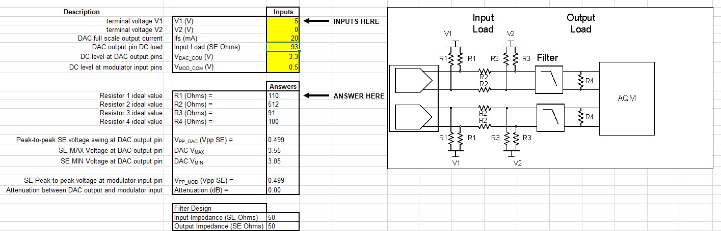
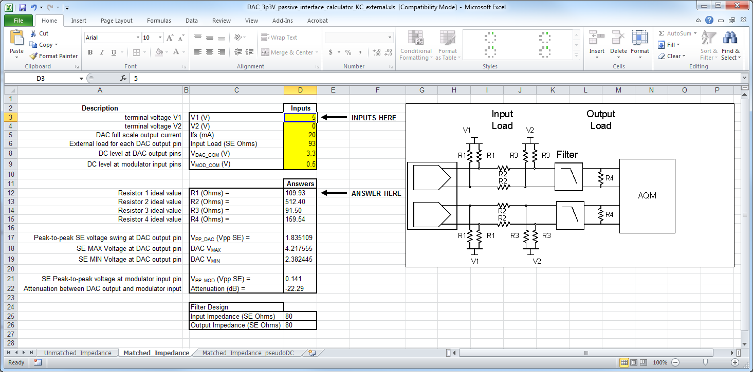
We are using the DAC3152 to drive a modulator (ADL5375) via a LPF. The interface between the is designed using the SLAA399 spreadsheet example to give
a DC offset at the DAC output and the modulator of 0.5 V with a single ended p-p voltage of 0.5 V.
For some reason we only see ~50 mV p-p as we generate a SSB signal at 4 MHz. Clock rate is 160 MHz.
I measured the bias resistor value (setting the maximum current) and it was populated correctly (~960R) which agrees with the designed 20 mA.
Any other ideas?
Thanks,
Johann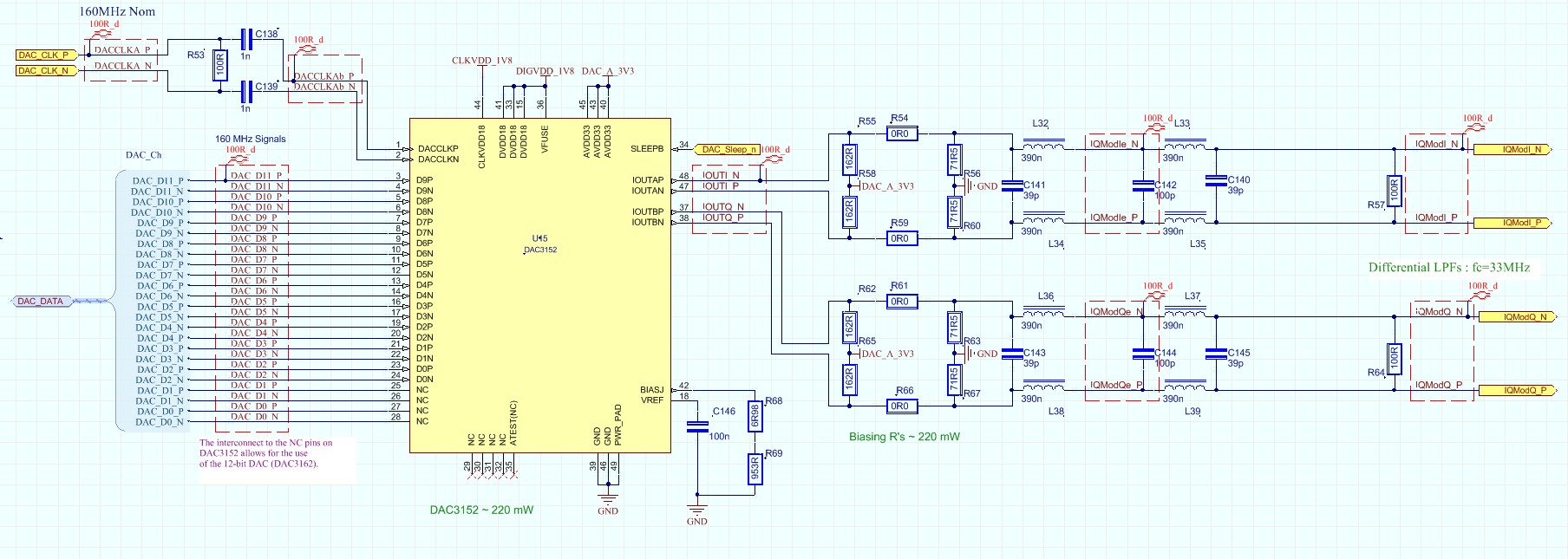


