This thread has been locked.

If you have a related question, please click the "Ask a related question" button in the top right corner. The newly created question will be automatically linked to this question.

JESD data corruption (KC705+ADC16DX370EVM)

Other Parts Discussed in Thread: ADC16DX370EVM, ADC16DX370

Hello!

I need some advice with using ADC16DX370. I'm trying to evaluate set of KC705+[optional TSW14J10]+ ADC16DX370EVM with Xilinx JESD core. 1 lane mode is used; ADC is controlled via TI's GUI. Link is successfully established; SYNC is high and stable. But received data are corrupted in a very strange manner. When ADC Test Pattern (0x70[2]) is enabled four values are repeated: -31032,0, 31032,0. It differs from [0, 26280, 0, –26328] declared in the ADC's datasheet.
When any JESD Test Pattern is enabled (ramp with step 1 for example) it produce chaotic data with weak track of true sequence.

Changing TX Driver parameters have no affects to link stability or data corruption. Enabling scrambler do not improve results also. I tried JESD cores 6.1 and 6.2 (Vivado 2015.2, 2015.3) at line frequencies 7.4Gbps (maximum allowed for ADC) and 4.0Gbps with same results. Reference clock for FPGA is 1/2 of sampling rate (1/40 of lane speed). It is generated at EVM board. Timing constraints in FPGA project are met.

Several examples of data for ramp mode with step =1 :

f8d3, f8d2, f8d1, f8cf, f8d0, f8ce,..

e3e3, e3fd, e3e5, e3fe, e3ff, e3e5, fd00, fd01, fd02,..

04b8, 04a6, 04a5, 04bb, 04a3, 04bd, 04be, 04bf, 0460, 0461, 0462, 047c, 0464, 047a

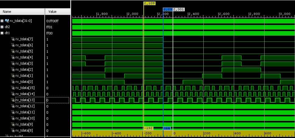
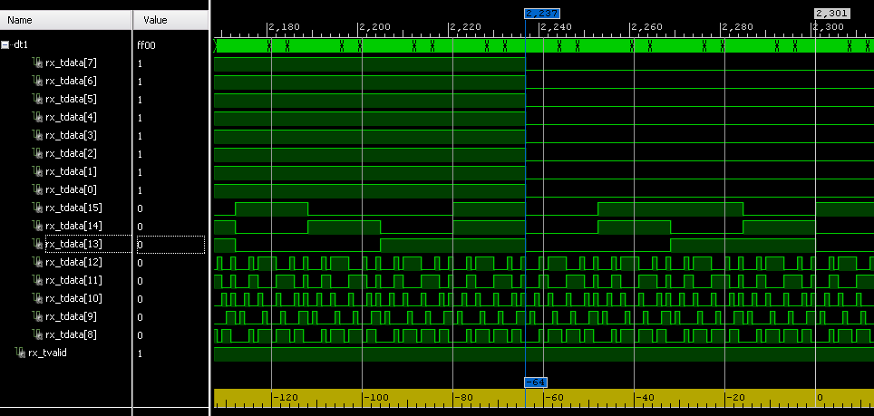
Examples of wave forms (with switching of high byte) is shown below

Please note that period of higher bits is power of 2 (64, 128, etc). They are not randomly changes at each sample. But they switches to incorrect values while counting. The only correct bit is 5 (it named as rx_tadata[13]).

So, it looks as parallel data corruption (not serial link corruption). Unfortunately I cannot determine the source of problem: ADC or Xilinx JESD core.

Could you make any suggestion, please? Thank you.

PS Important fact: same data sequence is repeated permanently. When Logic analyzer's trigger is set to any data value it captures same sequence everytime (for ramp pattern). For example:

ffe5, fffb, ffe3, fffd, fffe, ffff, 0000, 0001, 0002, 001c, 0004, 001a, 0019, 0007, 0008, 0016, ...

  • Alexey,

    It appears that the HSDC Pro software is incorrectly extracting the samples from the data stream. I'll set it up on the bench and see if I can reproduce.

    Regards, Josh

  • Alexey

    Please review the attached solution and let me know if it works for you. The .zip contains new custom files and has been tested with HSDC Pro v4.0

    Regards, Josh

    ADC16DX370EVM_TSW14J10EVM_KC705.zip

  • Some minor editorial updates to the procedure document:

    6354.ADC16DX370EVM_TSW14J10EVM_KC705.zip

  • Thank you very much. It works with some limitations:

    1) 2 lane configuration (421) works only. 1 lane configuration hangs HD Pro Gui for several seconds after pressing CAPTURE button.  Then the message "Read DDR to file TIMED_OUT_ERROR  Time out error" appears.

    2) My version of HSDC Pro v4.00.10 does not have embedded tab for ADC (EVM) configuration. I was need to start EVM GUI as independed program.


    Please note that my previous attempts did not include HSDC Pro software. I made my own simple FPGA project based on Xilinx JESD core with logic analyzer only. Today I Implement 2 lane configuration of my project and get similar results (LMK configuration from archive was used).

    So, I suppose following reasons of problem in my project:

    1) error data extraction from dataflow. Or additional encoding which applied to data somewhere. For ADC test pattern mode I got 0x0, 0x7938, 0x0, 0x86c8. The true sequence must be 0x0, 0x1928, 0x0, 0xe6d8 (I saw it in HSDC Pro today).

    2) Problems with core clocking which causes bit shifts or something like that.

  • Hmmm, I'll have to look at the 1-lane procedure again. It seemed to work yesterday. Maybe I wrote the procedure with an error. Anyhow, the 2-lane procedure gets you started

    For the test pattern, you should see (0x0, 0x66D8, 0x0, 0x9928) if the ADC is configured to output 2's complement and you should see (0x0, 0xE6D8, 0x0, 0x1928) if the ADC is configured to output offset binary.

    You are correct that the d/s incorrectly says that the pattern term is +26280. It should be +26328.

    I noticed the following about the characters you are receiving and the expected characters. If I take the 4-bit expected characters and match them up as best as possible to the characters you are getting, I can get the following. This shows that of your measured characters, the 1st, 3rd, 5th, 7th characters have an inverted 4th bit. So, it looks like the hex characters are jumbled up, and one of your bits in certain characters inverted. It might be interesting to switch the ADC output format and see which bit in the pattern get's inverted in the trasnsition between 2's and binary.

    Expected    Measured

    (9) 1001    1000 (8)

    (9) 1001    1001 (9)

    (2) 0010    0011 (3)

    (8) 1000    1000 (8)

    (6) 0110    0111 (7)

    (6) 0110    0110 (6)

    (D) 1101    1100 (C)

    (8) 1000    1000 (8)

  • Data format is another question. I found some inconsistency between ADC settings and real data in HSDC Pro:

    For 2's compl. format following sequence appears (I checked that bit DF 0x12[7] of ADC is 1). HSDC Pro shows values as unsigned numbers:

    32768, 6440, 32768, 59096 (0x8000, 0x1928, 0x8000, 0xe6d8). It's look like offset binary encoding (with central point at 0x8000)

    When offset binary format is set (bit DF 0x12[7] of ADC set to 0) I see

    0, 39208, 0, 26328 (0x0, 0x9928, 0x0, 0x66d8)

    Also I save binary ADC data via option File => Save Raw ADC codes as binary file. Results in binary file are corresponding to values above.

    I made screenshot of GUI when 2's comlement mode is set. May be I made something globally wrong?

  • Further, about my own project. For ADC test mode I got

    0x0, 0x7938, 0x0, 0x86c8 when 2's complement mode is used and

    0x8000, 0xf938, 0x8000, 0x06c8 for offset binary mode.

    Unfortunately it is not possible to switch between 2's and OB for ramp test. Data format is selected by ADC core but ramp is generated inside ADC's JESD interface.

    You made very interesting observation about data bit mixing. I'll try to analyze it with bigger data set.

  • Please note that there is a post-processing step that the HSDC Pro software performs after it receives the data from hardware but before the data is displayed. The post processing function is stored in a EVM-specific configuration file located at \{HSDC Pro Install DIrectory}\{Data Capture Board Name}\{ADC Name}.ini. For the ADC16DX370, the post processing step is to invert the MSB. The default format of the ADC16DX370 is 2's compliment, so this post processing converts to offset binary so that it can more easily be converted to decimal and analyzed. So, keep in mind that HSDC Pro will always show you data with the MSB inverted.

    Regards, Josh

  • Thank you for notice about MSB inversion. It clears GUI results.

    I made full ramp table of codes captured by logic analyzer. May be it interesting. First column is ramp 0..65536; second column is actual code received from JESD. Both in hex.jesd_bit_mix.csv.zip

  • Finally, I wrote simple conversion module. It consist of 8-bit look-up-table. Each octet from JESD should be converted with the module. As a result, I got fine signals from ADC: ramp as well as sine signals from RF generator.

    Unfortunately, I have no ideas about reasons of that data modifications.

    jesd_octet_lut.vhd.zip