This thread has been locked.
If you have a related question, please click the "Ask a related question" button in the top right corner. The newly created question will be automatically linked to this question.
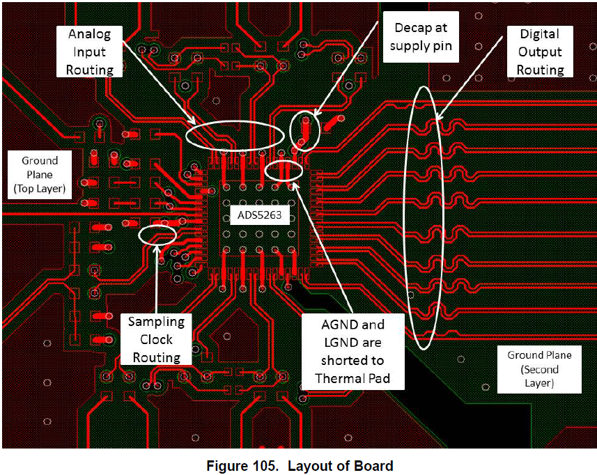
What ground wiring pattern do you recommend? "Figure 105. Layout of Board", p.73 of ads5263's datasheet shows common ground plane both for analog (AGND), digital (LGND) ground pads of ads5263. We are considering to split them into 2 ground planes, connected at one point in order to reduce interference between digital signals and analog part of ADC. Would you recommend such practice and where should we connect those ground nets to each other?
Hi Anton,
Thanks for using our ADS5263 device.
We will look into your questions.
And we will replay to you soon.
Thank you!
Best regards,
Chen
Hello Anton,
How are you?
Thanks for using our ADS5263EVM.
To separate AGND and DGND, our ADS5263EVM uses 2nd layer as the ground plane
and split it into left (as AGND) and right (as DGND) portions except at the center part of the plane (connected).
Please look at the following:
If you zoom in the above plot, then 1st layer and 2nd layer are shown together:
1st layout shows analog input signals including clock-in (on the left hand side) and digital output signal (on the right hand side).
Thank you very much.
Best regards,
Chen