This thread has been locked.

If you have a related question, please click the "Ask a related question" button in the top right corner. The newly created question will be automatically linked to this question.

ADS1248 - Spikes when toggling Vref

Other Parts Discussed in Thread: ADS1248

Hello,


we observe random spikes in the acquired data from ADS1248, which we need to debug and eliminate.

Circuit:

Our application is thermocouple temperature measurement, we use two channels of the ADS1248 chip one for a voltage measurement of a thermocouple, for that we use external voltage reference of 2.048V, other channel for a cold junction temperature measurement (a thermistor) where we use ratiometric technique using a precision resistor as a reference and the IEXC current source of 100uA (always enabled). The reference voltage generated across the reference resistor is about 0.62V (a resistor is 6.2k). During the acquisition we continuously change:

1) ASD1248 Input channel (a thermocouple or a CJ thermistor)

2) Gain (G=16 for a thermocouple and G=1 for a CJ)

3) Voltage reference (external Vref1 of 2.048V for thermocouple and external Vref0 of about 0.62V for the CJ)

The application is similar to that described in the ADS1248 datasheet (SBAS426H from March 2016) "10.2.2 K-Type Thermocouple Measurement (–200°C to +1250°C) with Cold-Junction Compensation".

The acquisition cycles single measurements of a thermocouple channel or a thermistor channel after previously configuring that channel followed by the SYNC command. We use Data out as DRDY mode and "read data continuously" to make that mode possible. The ADS1248 is powered from unipolar power supply of 3.3V. Internal voltage reference is always turned on to allow the IEXC current. The data from ADS1248 are retrieved immediately after detecting DRDY condition so DRDY does not corrupt Data stream. We use the internal clock of the ADS1248 which runs the modulator of the chip. The chip is never powered down nor enter a sleep mode.

Problem:

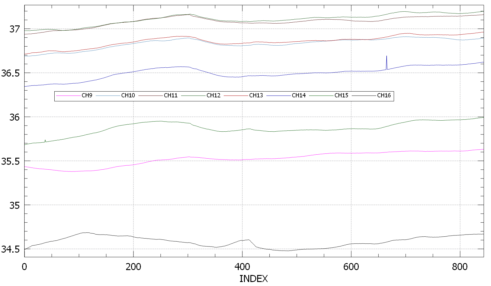
In general our circuit works, we use multiple identical channels (multiple ADS1248 chips on one board) and both thermocouple voltage and the thermistor resistance can be measured correctly at various acquisition speeds. The problem with corrupted data occurs randomly. Sometimes a ratiometric measurement of a thermistor resistance is not correct and when plotted looks like a spike, it can be in either direction, amplitude of anomaly is also random. A plot shows a single spike present on channel14 (a blue trace). The problem occurs at various ADS1248 speeds including the slowest of 5SPS. Analysed RAW (binary) ADC data do not suggest any particular communication issue.

Findings:

We tried many different configurations to narrow possible causes of the spikes on the CJ channel we observe. We noticed that toggling voltage reference between measurements (we need to do it as we measure voltage of the thermocouple and a resistance of the thermistor) influences it. When the voltage reference stays always the same (either external Vref0 or external Vref1 or internal) then the spikes are not present. Also when the Voltage reference is toggled between external Vref1 of 2.048V and the internal one of 2.048V the spikes are not present. In addition when the external voltage reference generated across RRef is increased from 0.62V (100uA*6.2k) to 1.55V (250uA*6.2k) the spikes are not present. When the external voltage reference generated across RRef is reduced to 0.3V (50uA*6.2k) the spikes are happening more often. We tried to introduce a delay after changing a voltage reference source and before performing the measurement but the spikes were still observed.

Questions:

What may cause the problem with spikes we observe?

Is there any restriction of amplitude of voltage reference when it is changed between measurements?

The ADS1248 data sheet says that recommended minimum amplitude of external Vref is 0.5V (parameter moved in the newest data sheet from electrical characteristics to recommended characteristics). Can ADS1248 operate with external Vref lower that 0.5V?

Is there any particular time needed after changing a voltage reference source (other than 32 modulator clocks ADS1248 imposes after accessing the MUX1 register)?

Regards,

Robert
  • Robert,


    Thanks for the detailed writeup of your problem.

    My first thought was that there is some sort of delay in the use of the reference. This could be as simple as extra capacitance on the reference and a changing value as the reference settled. If you are switching the IDAC to a new channel and there's a large capacitance on the reference resistor, then there's some settling time involved as the IDAC current fills the capacitance. This also applies to the measurement input as well. If the input filtering is large, then it may take extra time to settle the measurement.

    You might want to check the measurement when you remove any capacitance from the reference or input of the ADC. This might eliminate this as a problem. Also, changing the data rate may chance the nature of this problem also. With a slower data rate, the time needed to settle would stay the same and be a smaller spike in the measurement.

    However, since you included the delay and you still see the problem, it might not be the settling. Also, changing the data rate and seeing a similar spike is also suspicious. Still, I'd go through some of the above tests just to see if there is a change. I'd also try looking at the voltages through an oscilloscope, just to see if the voltages settle quickly.

    I'd also check to make sure that when the reference is in, it does not get routed to the REFP0 and REFN0 pins. This is done in the MUX0 register with bits 4:3. If you are changing this register,

    If you have the raw binary data, I'd prefer to look at that. Is it possible to get it in an excel spreadsheet format? I'd need to know what you are measuring, what voltages are expected for input and references, and the setup (including the data rate and the routing of the IDAC voltages). I'd also like to know the amplitude of the spike at different data rates and different delays. Does the spike change with any of these modifications? What is the time scale of the graph you provided?

    At some point, it might be nice to have a schematic (or partial schematic) to help with the debug. If you are not able to post one, perhaps we can make contact through email.

    Looking through your questions, I'll just go through the answers individually.

    1. There shouldn't be any restriction on the amplitude voltage of the reference except for perhaps the maximum voltage of (AVDD-AVSS-1V).

    2. I believe that the minimum amplitude of the VREF voltage of 0.5V was a bit of an arbitrary selection. I'll need to confirm that with the design group (I believe actual the designer is out on vacation though). I'm not aware of any part of the internal circuitry that would prevent the operation at that low of a voltage.

    3. Generally the time needed after changing the voltage reference source should be low enough to use the next data. The exception to this is any delay in settling of the measurement from something external to the ADS1248. As mentioned before, this is usually high capacitance at the inputs or reference voltages as something has switched or changed and needs to settle.

    As I mentioned earlier, I'm not sure what the source of the problem is. However, read through my comments, run a few tests and perhaps we can come up with something.


    Joseph Wu
  • Joseph,

    thank you very much for a fast response and tons of ideas. I will perform additional tests, in the mean time I will add some missing information. Maybe it will suggest you something.

    Joseph Wu said:
    My first thought was that there is some sort of delay in the use of the reference. This could be as simple as extra capacitance on the reference and a changing value as the reference settled. If you are switching the IDAC to a new channel and there's a large capacitance on the reference resistor, then there's some settling time involved as the IDAC current fills the capacitance. This also applies to the measurement input as well. If the input filtering is large, then it may take extra time to settle the measurement.

    Actually at the reference resistor there is no any capacitance (beside parasitics). We tried to add a capacitance across RRef to see an effect but the spikes we still observed. The ADC input is another resistor (a thermistor) also without any onboard capacitance (we also tried adding one without any effect). The excitation current goes trough IEXC1 dedicated pin, it is enabled before an acquisition and stays at that state all the time, so the voltage across a reference reference resistor is constant all the time, the same for the sensor. They are both located close to ADS1248. The reference resistor is 6200 Ohms so the voltage across it is 620mV at IDAC of 100uA, the sensor resistance is about 1800 Ohms at 30oC so the voltage across it 180mV. The compliance voltage if the IDAC is maintained (620mV+180mV=800mV well below VCC of 3.3V).

    Joseph Wu said:
    You might want to check the measurement when you remove any capacitance from the reference or input of the ADC. This might eliminate this as a problem. Also, changing the data rate may chance the nature of this problem also. With a slower data rate, the time needed to settle would stay the same and be a smaller spike in the measurement.

    The spikes are random in amplitude. I have not noticed (yet) any relation of sampling rate relation to ADC sampling speed. It might be that ADC speed affects how often they appear. Some settings cause that the spikes disappear temporarily so it it very difficult to conclude anything for sure.

    Joseph Wu said:

    However, since you included the delay and you still see the problem, it might not be the settling. Also, changing the data rate and seeing a similar spike is also suspicious. Still, I'd go through some of the above tests just to see if there is a change. I'd also try looking at the voltages through an oscilloscope, just to see if the voltages settle quickly.

    The measured and reference voltages are (almost) constant all the time, only the input channel of the ADC changes along with its configuration settings. There is no any onboard settling, only the settling internal to the ADC itself.

    Joseph Wu said:

    I'd also check to make sure that when the reference is in, it does not get routed to the REFP0 and REFN0 pins. This is done in the MUX0 register with bits 4:3. If you are changing this register,

    I think you meant MUX1 register. Yes this register is changed before each measurement but it is never enabled to direct the internal Vref to REF0 pins. It uses only 00b for external REF0 input or 01b for external REF1 input. Some tests were also performed with 10b for the internal Vref.

    Joseph Wu said:

    If you have the raw binary data, I'd prefer to look at that. Is it possible to get it in an excel spreadsheet format? I'd need to know what you are measuring, what voltages are expected for input and references, and the set-up (including the data rate and the routing of the IDAC voltages). I'd also like to know the amplitude of the spike at different data rates and different delays. Does the spike change with any of these modifications? What is the time scale of the graph you provided?

    I will try to attach an Excel document and a related graph. It is the acquisition run with ADC_SPEED of 160 SPS (this is how the ADC is configured) but single samples are collected with 10SPS (this is how often ADC is asked to do a measurement). The acquisition shows number of spikes with different amplitudes using the same settings. About 16000 samples from 16 different ADS1248s all located on one board were collected , about 30 minutes of the acquisition time. After each ADC command an extra delay of 2000us was added in this test. The ADC measures two channels (voltage of a thermocouple and a resistance of a thermistor) but only data of one channel are logged, the one which shows spikes and uses the ratiometric method to measure a resistance of a sensor. The  vertical scale is a calculated temperature of the sensor (36oC translates to about 1400Ohms what is about 1/4 of the reference resistor of 6200Ohms). Obviously even in ratiometric configuration ADC measures voltages so Vref is 6200R*100uA=620mV, ADC input is about 1400R*100uA=140mV

    116 at 10SPS 100uA ADC_SPEED160 SEQ_DELAY2000.xlsx


    Joseph Wu said:
    At some point, it might be nice to have a schematic (or partial schematic) to help with the debug. If you are not able to post one, perhaps we can make contact through email.

    If possible I can post a schematics by email.

    Regards,

    Robert

  • Robert,


    Thanks for putting up the data. I've gone through it, looking at the errors, but I'm still not sure what the problem is.

    At first, the data looked like it might be a communication problem, but I'd it's probably not that for a couple of reasons.

    First, you see this issue most on channels 1 and 4. On the other channels, you see it a couple of times, on a little more than half of the channels, you don't see it at all. Generally a communication issue would be randomly spaced through all the channels (unless there were unusual circumstances in the setup and data order. Second, it doesn't line up with common communication problems that I've seen in the past. If it were a delayed read from a /DRDY indication (and an interruption from a new /DRDY), you'd see that in the raw data with the second start of a read within the data word. Another communication error would be noise on the SCLK line, advancing the data read. This would often make the data larger, and here it appears to always make the data smaller (I'd note that you could still test this out by adding some capacitance to SCLK to try to eliminate the noise). In addition to the other comments from yesterday, it's unlikely this is a communications error.

    Looking at the data, the errors from the readout always show the signal as smaller. In this case, it means either the signal really is smaller, or the reference is getting larger during the read.

    Since the errors are different channel to channel, is it possible this error is EMI related? Are the sensors in different physical locations where they may be more susceptible to interference? If so, can they be shielded?

    Are you using some sort of external multiplexer? There are 16 channels of data, and that wouldn't be possible with the device's on-board mux. The added circuitry may make readouts and changing channels more complicated.

    Also, is there some way to do multiple readouts of data for each channel? I would just check to see if you get the same error if you do two reads and throw out the first read. Or you could record multiple readings for each channel to see if the error remains or settles back to normal. (Right now I'm assuming that you read out channels 1 through 16 repeatedly)

    Regardless, I've put out a friend request through the E2E system to you. Connect with me and you'll be able to send me a schematic without posting it.


    Joseph Wu
  • Joseph,

    thank you for your replay. A short question first: how to send a private message to you?

    Joseph Wu said:
    First, you see this issue most on channels 1 and 4. On the other channels, you see it a couple of times, on a little more than half of the channels, you don't see it at all.

    That is a correct observation but only for the particular acquisition I sent, I think that it happens on all channels. In general I could work with one channel only, but you correctly noticed that some channels are quiet, sometimes I have to wait even hours to get a spike and sometimes there is a flood of spikes. At first I thought it is temperature dependent but I am not sure any more.

    Joseph Wu said:
    (I'd note that you could still test this out by adding some capacitance to SCLK to try to eliminate the noise)

    The SI quality of signals have been already optimized, a special care was put into mentioned SCLK signals (crucial for a synchronous interface) at design level and during optimizing a prototype. Until problem is known I do not exclude anything even things which seem to be solid. The scope picture below shows how the SCLK signal edges look like after optimizing the SI terminations (monotonic, no excessive ringing). In addition long term interface tests were run by writing various data to the ADS1248 register (including PRBS patterns to catch possible ISI) and read it back, communication works correctly.

    Joseph Wu said:
    Looking at the data, the errors from the readout always show the signal as smaller. In this case, it means either the signal really is smaller, or the reference is getting larger during the read.

    It is not always the case, I wrote before that the spike can be in either direction. I have to admit that during one acquisition (set of settings) most of spikes are in one direction (either up or down) what may be an important clue. Below there is a plot showing spikes in both directions even looking at a single channel.


    Joseph Wu said:
    Since the errors are different channel to channel, is it possible this error is EMI related? Are the sensors in different physical locations where they may be more susceptible to interference? If so, can they be shielded?

    Anything is possible until we find out what the problem is. The sensors are local, close to ADCs and all channels are identical. The instrument is covered by a metal enclosure, the effect of spikes is observed with that enclosure and without it. Remote thermocouple sensors were replaced by a local short to exclude one variable.

    Joseph Wu said:
    Are you using some sort of external multiplexer? There are 16 channels of data, and that wouldn't be possible with the device's on-board mux. The added circuitry may make readouts and changing channels more complicated.

    No, there is no any external multiplexer, I wrote before that we use multiple ADS1248 on one board. I can run up to 48 of ADS1248 simultaneously (one instrument), I could synchronize several instruments with uncertainty below 100ns if necessary (IEEE1588). I would prefer to work with one channel only, modify then test, modify then test... The problem is that sometimes (as you previously noticed) some channels are quiet, running more channels (I mean several ADS1248s) simultaneously we have more chance to have a spike and to abandon the particular fix. How to prove that the problem is solved? I have no idea, sometimes measurements are promising and a single spike after number of hours ruins the idea (like below).

    Joseph Wu said:
    Also, is there some way to do multiple readouts of data for each channel? I would just check to see if you get the same error if you do two reads and throw out the first read. Or you could record multiple readings for each channel to see if the error remains or settles back to normal.

    That is a very good idea (for a test only not as a solution because we do not have enough time between measurements). I will think how we can perform that test. What I want to achieve is to configure a channel, let the ADC reset its filters, do the first measurement after changing the configuration (wait for the first DRDY after changing the configuration) and get the ADC code of the same measurement twice. We do not have much flexibility because ADS1248 is connected to the FPGA not to a uC, so changes are possible but time consuming.

    Alternatively I could do series of two measurements after changing the ADC configuration to see if the second one recovers to a correct value, I think it does. Previously I tried to add a (ridiculous) delay longer than the ADC measurement so the ADC did not return the very first measurement after changing a configuration but some later and there were no spikes. I think that the very first measurement after changing Vref is sometimes corrupted.

    Joseph Wu said:
    (Right now I'm assuming that you read out channels 1 through 16 repeatedly)

    Simultaneously as we have many ADS1248 chips on one board. One ADS1248 uses its two local channels, which are multiplexed, one for voltage measurement second for ratiometric resistance measurement, and the two internal channels of each ADS1248 are measured sequentially using the internal ADS1248 multiplexer. Together with the ADS1248 channel we need to set up (change) gain and the voltage reference source. I believe that changing the voltage reference causes the trouble. I tried: to not to change gain=spikes, to not to multiplex the internal ADS1248 channel and measure only the NTC sensor using both voltage references=spikes, then to measure both a voltage of one ADS1248 channel and a resistance using another ADS1248 channel from ONLY one voltage reference (either RRef or an external VREF0 or the internal one) and I observed no single spike.

    In addition I believe that it has to do something with the amplitude of the voltage reference, so I asked whether there are any restrictions. When I increased the voltage across RRef (normally it is 6200R*100uA=0.62V) to 1.5V the spikes have gone (I increased the excitation current from 100uA to 250uA). I also tried to increase that voltage by doubling the RRef resistance and staying with the same 100uA current, the spikes were also gone. Then I simply tried to reduce voltage across RRef by changing the current to 50uA (6200R*50uA=310mV) and the spikes were exaggerated.


    Regards,

    Robert

  • Robert,

    To connect, you should have gotten a message from me through E2E. If you go to the icons in the upper right corner of the E2E site, you'll see notices.

    It's strange that there is such an intermittent nature to the problem. I find that it'll be useful to keep it in some mode that has he problem, so keeping the VREF low may be useful.

    Looking at the SI quality may not tell you much if the error source is comes from some sort of EMI spike. Since the error is intermittent (in the one sent to me ~5 per 16000 readings) you need to catch something that is a fairly rare event.

    In the first plot of the last post, I can see that it does have some up/down spikes. If you can capture a few of those and send that to me in excel, I can look at that data too. Perhaps there's two different errors occurring. Also the last plot of the post, there are lots of errors. I'd like to get that one too. Just as a qualitative look at these posts. Some channels have a high correllation to other channels. Also in some of these errors, the errors are similar in magnitude. In the last plot, you can see this in some of the channels, and it might be nice to get the data for that one in particular.

    Joseph Wu

  • Joseph,

    thank you for the reply.

    Joseph Wu said:
    To connect, you should have gotten a message from me through E2E. If you go to the icons in the upper right corner of the E2E site, you'll see notices.

    I have added you yesterday as my E2E friend but I still do not know how to send you a private message. Have you added me too? Do you have the messages enabled?

    https://e2e.ti.com/group/helpcentral/f/301/t/190481

    After your suggestion I run two additional tests, where data were read twice.

    A) REPEATED READING

    The ADC channel was configured (Vref changed to RRef) and the very first conversion was read from ADS1248 twice using two RDATA commands (the same conversion from the ADC). The spikes were caught, the same spikes were get from the ADC twice. Basically ADC returned two values of exactly the same code. In my opinion it significantly reduces chances that there is something wrong with the interface.

    REPEATED READ.xlsx


    B) REPEATED MEASUREMENT

    I also managed to read first two conversions after changing Vref to RRef (a change of the configuration and then two ADC conversions without touching the ADC settings). I read two values of very similar code, as the conversions were performed immaterially one after another, they (normally) differ at the level of a noise. The spikes were also acquired and I have the following observations:

    - if the first conversion was without a spike, the second was also correct

    - if the first conversion was with a spike, the second is sometimes correct

    - if the first conversion was with a spike, the second is sometimes with a spike of the same amplitude (+/- noise)

    - if the first conversion was with a spike, the second is sometimes with a spike of reduced amplitude and the same direction

    - if the first conversion was with a spike, the second is sometimes with a spike of reduced amplitude and an opposite direction

    So, if there is a spike the ADC does not recover within one conversion.

    Joseph Wu said:
    In the first plot of the last post, I can see that it does have some up/down spikes. If you can capture a few of those and send that to me in excel, I can look at that data too.

    I captured one channel with up/down spikes, a part of a long acquisition is in the Excel document (one channel only).

    Spikes in both directions.xlsx

    Joseph Wu said:
    Some channels have a high correllation to other channels. Also in some of these errors, the errors are similar in magnitude.

    I noticed that too, sometimes it looks like spikes are approaching a particular level. Please notice that vertical scale is temperature of a sensor, as the sensor is close to the ADC it somehow reflects temperature of the chip as well. When temperature changes intensity of spikes changes as well, that is why I thought that temperature affects the issue. Actually I think (a theory only) that it possibly does but indirectly: temperature affects significantly a frequency of the internal oscillator of the ASD1248 (manifests by extending or shortening distance form a start of conversion to DRDY, the internal clock cannot be observed directly). The measurements in our application are requested asynchronously to the internal clock of the ADC, it might be that at some temperatures probability of the spike effect is higher as relation between the internal ADC clock and the asynchronous conversion request (SYNC command in our case) favours it.

    REPEATED MEASUREMENT(CH5).xlsx

    Joseph, is there any chance that you try to reproduce the issue on your side? Are you able to control (switch) the ADS1248 configuration and to acquire the very first conversion after changing a configuration?

    Regards,

    Robert

  • Robert,


    Thanks for the last set of data, it'll take me some time to look through this, but I'll do what I can.

    I've sent you an E2E message with my email address. This way you can send me a schematic and you can send me some more detailed information about the circuit. Look for the notice at the upper left corner of the browser window when looking at the E2E pages (as I indicated in my last post).

    I'm not sure I can duplicate your data taking process. I'm quite sure that plenty have done this sort of channel cycling without problems and have made configuration changes all the way up to 2kSPS without running into a similar issue. I just don't have a fixture that can take this data with any kind of programming.

    Regardless, with my email you should be able to get some more detailed information to me.


    Joseph Wu
  • Robert,


    Thanks for your email. I've had a chance to look over your schematic and I do have a few comments and questions.

    First, I would remove L1.1 and replace it with a short. Often, inductances in the supply will cause a large ringing in digital supplies, In this case, DVDD or the IGND is causing large voltage changes that can affect the performance of the circuit. I know it's there as a filter, but with digital circuits, it can also look a little like a resonator.

    What is your SPI clock rate? If you have any timing violations, you might see errors in communication. If you can, try to get a scope shot to verify the digital communication (SCLK, DIN, DOUT, and /CS)

    I would also try to add some capacitance to VREF0 and VREF1 to see if the problem gets better or worse. At this point, you seem to have the most problem as VREF transitions from one voltage to another voltage. This might be an added test.

    For the data you are reading, is this the raw data coming out of the part? Or is this converted from the readings that you are getting? I want to know because aspects of this problem looks like a digital communication issue. I'd try to remove the isolation and make sure that you get the same issue, I'd also try to use a logic analyzer to make sure that the data coming out of the part itself is matching the reading.

    One last thing that I had as a concern was if there were any cases where the input is over-ranging. Consider cases where the input reading one thing, and then the reference changes to something very small. In this case, the input may have over-ranged the ADC modulator and may take extra time to recover. There may be other cases where you have the measurement in gain, and then you switch to a larger input, where the gain is no longer needed and you've over-ranged the input PGA. This may also require extra time to recover.

    Regardless, read through my comments and there should be a few things to test. Let me know what you think and any results that you come up with.


    Joseph Wu
  • Joseph,


    thank you for your comments and a next handful of ideas.

    Joseph Wu said:
    First, I would remove L1.1 and replace it with a short. Often, inductances in the supply will cause a large ringing in digital supplies, In this case, DVDD or the IGND is causing large voltage changes that can affect the performance of the circuit. I know it's there as a filter, but with digital circuits, it can also look a little like a resonator.

    That is true, but it is not a cause of the problems. It was tested with a 0R short instead of the L1.1 inductor (actually a ferrite) and also using a 12R resistor. In all cases the spikes are present. Local supplies AVDD/DVDD were also observed and no excessive noise was detected. It is a bit inconvenient to (correctly) monitor the supplies as a normal circuit current is a few mA and appropriate 50R probe would load the circuit far more. I used a high impedance probe which normally picks up more noise than there is in reality in the circuit but even then the supplies were clean and the spikes observed. As the spikes are random and happen not too often it is difficult to correlate the actual supply oscilloscope measurement to a moment when a spike happened. I can say, that the supplies are clean even when monitored over some longer time.

    Joseph Wu said:
    What is your SPI clock rate? If you have any timing violations, you might see errors in communication. If you can, try to get a scope shot to verify the digital communication (SCLK, DIN, DOUT, and /CS)

    There is possible to vary the SPI clock within some limits. Normally the SPI clock frequency is 500kHz. A timing of the interface towards the ADS1248 and in the opposite direction was verified on the scope.

    Joseph Wu said:
    I would also try to add some capacitance to VREF0 and VREF1 to see if the problem gets better or worse. At this point, you seem to have the most problem as VREF transitions from one voltage to another voltage. This might be an added test.

    I wrote before that we tried to add a capacitance across a reference resistor RRef (Vref0), it does not help. At Vref1 we have not tried, but instead we used the internal one together with the Vref0, we tried some capacitance values of C1.9 (internal Vref bypassing) and the spikes were present.

    Joseph Wu said:
    For the data you are reading, is this the raw data coming out of the part? Or is this converted from the readings that you are getting? I want to know because aspects of this problem looks like a digital communication issue. I'd try to remove the isolation and make sure that you get the same issue, I'd also try to use a logic analyzer to make sure that the data coming out of the part itself is matching the reading.

    The data I sent were RAW data from the ADC. Internal ADS1248 offset registers are cleared, gain registers are untouched (factory calibrated as I understand).

    We also tried without the isolation, spikes were still present. It is not easy to catch the corrupted data on a scope/logic analyzer.

    For me it does not like a digital communication issue:

     -depending of the Vref configuration the spikes can happen often, rarely, or disappear completely (how to prove it?)

    - if the ADC is asked a second time for the same data within a single conversion (repeated RDATA) it returns exactly the same code (with a spike or without a spike)

    Joseph Wu said:
    One last thing that I had as a concern was if there were any cases where the input is over-ranging. Consider cases where the input reading one thing, and then the reference changes to something very small. In this case, the input may have over-ranged the ADC modulator and may take extra time to recover. There may be other cases where you have the measurement in gain, and then you switch to a larger input, where the gain is no longer needed and you've over-ranged the input PGA. This may also require extra time to recover.

    Very good thought. It was actually the very first idea we analysed. Documentation to the ADS1248 mentions that overload shall be avoided. To eliminate overload condition we use a particular order of commands:

    1) Select a thermocouple input AIN0-AIN1

    2) Change to PGA=16 and Vref1=2V (one WREG command to two registers)

    Take a single measurement

    3) Change to PGA=1 and Vref0=0.6V (one WREG command to two registers)

    4) Select a thermistor input AIN2-AIN3

    Take a measurement and start from the beginning

    -------------------------------------------

    That order shall avoid the overload state at least from the ADC input perspective. To further minimise a possibility of overload we tried:

    - to provide an external short to a thermocouple channel AIN0-AIN1 (voltage always 0V (+offset+noise))

    - additionally to not to toggle the gain and in the stage 2 it was also PGA=1

    - in addition to not to change the input and it was always a thermistor (AIN2-AIN3)

    In all cases the spikes were present if only Vref was changed from 2V to 0.6V. If the Vref was not changed (another test(s)) and it was always either 2.048V or constantly 0.6V no a single spike was observed.

    Maybe the issue is related (or similar) to overload condition not at the ADC input but rather from Vref side and internal circuits get unstable. How such instability  caused by overloading inputs looks like? Last time I sent some results showing two consecutive measurement taken from each ADC channel, I observed that sometimes the spike is present in the second measurement, usually of a lower amplitude, sometimes in an opposite direction to the expected value than the first spike. Can it suggest some internal instability of the chopper?

    Regards,

    Robert

  • Robert,


    We've been discussing the problem you've seen here and we think that the problem isn't a case of the reference being small, but rather the input being on the edge of the common mode range and similar to the fact that you may be over-ranging the input. We've seen something like this before, but usually when the problem is seen, it's a more consistent effect. However, for your case, you might be on the edge of the problem.

    There are two things that you might be able to try to limit this effect.

    First, when you make the change from measuring the thermocouple to measuring the CJ thermistor/rtd, split the command to make the change into two commands. When the part is receiving the command to change the registers, the change occurs as the new register value is decoded (i.e. in order of the register address). By sending the information as one command, the mux input is set first, followed by the reference input, then the PGA and data rate settings.

    If you start out measuring the thermocouple (which is measuring in a gain of 16) and then go to measuring you set the CJ thermistor/rtd, the first thing it does is switches the input, but keeps momentarily keeps the device in a gain of 16, which may over-range the input, or push you out of your common-mode range.

    Instead, when you switch from the thermocouple measurement, first set the PGA to 1. Then go back and set the mux input. By setting this as two commands, you avoid the over-range condition.

    The second thing that might work is to raise the input common-mode range to see if the problem goes away. Right now, the reference resistor also sets the input common-mode voltage of the measurement. You can add a second resistor below the reference resistor to act as a pedestal voltage, raising the input common-mode. This way you can use the same reference resistor, but since this stack adds to the voltage underneath the input voltage, it raises the common-mode.

    I'd note this might take some board surgery, but it might not be that difficult to test. If you air-wired the reference and a second resistor to ground, you'd be able to look at this quickly.

    Regardless, let me know what you think.


    Joseph Wu
  • Robert,


    Just to let you know, I did talk to a couple of the designers about low VREF operation and they didn't think it would have many consequences. We do put a lower limit on the reference of 0.5V, but in general, that's to keep the up the performance with noise and offset. There shouldn't be any issues with stability from either the modulator or any kind of chopping.

    Regardless, I think the method I mentioned in the last post should be fine to test. I suspect they would clear up the problem you're seeing. It seems that this measurement problem is the right transition from high to low reference (and therefore PGA transition) to show the problems you're seeing. Again, make the modifications and see if it helps.


    Joseph Wu
  • Joseph,

    thank you again for your support. Unfortunately the problem is still present. I put some comments and new observations below.

    Joseph Wu said:
    First, when you make the change from measuring the thermocouple to measuring the CJ thermistor/rtd, split the command to make the change into two commands. When the part is receiving the command to change the registers, the change occurs as the new register value is decoded (i.e. in order of the register address). By sending the information as one command, the mux input is set first, followed by the reference input, then the PGA and data rate settings.


    We do exactly this: channel selection and Vref/PGA/Speed selection are done in two separate commands. Please look at my previous post, the order (a channel selection before a PGA selection or vice versa) is different whether we change CJ to TC or TC to CJ. It is to avoid overloading the PGA.


    In addition to narrow possible causes I made some tests as explained before (e.g. to not to change the PGA (always 1) or to not to change the ADC channel (to not to use AIN0-AIN1 for the TC even the TC was temporarily shorted), the spikes were still in place if only Vref was changed between measurements.

    Joseph Wu said:
    The second thing that might work is to raise the input common-mode range to see if the problem goes away. Right now, the reference resistor also sets the input common-mode voltage of the measurement. You can add a second resistor below the reference resistor to act as a pedestal voltage, raising the input common-mode. This way you can use the same reference resistor, but since this stack adds to the voltage underneath the input voltage, it raises the common-mode.

    This is an interesting possibility so I spent a bit more time around the possible solution. Unfortunately it did not helped. Amount of spikes is similar whether VrefN0 is at GND potential or elevated. I tested the following possibilities (in addition to previous tests):

    VrefN0 was elevated to 0.5V using the 10k extra resistor and 50uA excitation current, Vref0 was ~300mV (to be precise everything was elevated by 0.5V Vref and AIN)

    VrefN0 was elevated to 1V using the 10k extra resistor and 100uA excitation current, Vref0 was ~600mV

    VrefN0 was elevated to 1V using the 20k extra resistor and 50uA excitation current, Vref0 was ~300mV

    VrefN0 was elevated to 2V using the 20k extra resistor and 100uA excitation current, Vref0 was ~600mV

    In all 4 cases the spikes were present similar as without rising the Vref. There is much difference whether Vref0 is 300mV (a lot of spikes at all ADC speeds), 600mV (seldom spikes and at some ADC speeds only), 1V (no spike observed so far).

    ---------------------

    In addition I performed the following tests: Vref0 was 300mV or 600mV (Vref voltage where spikes are observed) and I limited Vref1 to about 1V and to about 0.5V. I thought that the difference between voltage references causes the problem, but the same amount of spikes was observed for all voltages of the Vref1.

    A next test was to use an external pull-up to the +3.3V instead of the excitation current from the ADC (50uA or 100uA). The pull-up was selected to build across the RRef (R10) of 6.2k about 600mV and the spikes were observed as before. A stronger pull-up was then used to build across RRef about 1V and the spikes were not observed any more. I still believe that low amplitude of Vref0 causes the issue. If amplitude is raised up either by using a higher value of Rref or by using a higher current of IEXC or by using an external pull-up instead of IEXC reduces or possibly eliminates the spikes.

    Regards,

    Robert