Because of the Thanksgiving holiday in the U.S., TI E2E™ design support forum responses may be delayed from November 25 through December 2. Thank you for your patience.

This thread has been locked.

If you have a related question, please click the "Ask a related question" button in the top right corner. The newly created question will be automatically linked to this question.

Sending sine wave pattern from Xilinx KC705 to DAC37J82 results in noisy data output on analog line

Other Parts Discussed in Thread: DAC37J82, LMK04828

Hi all,


I’m using the Xilinx KC705 EVM and TI DAC37J82 EVM to evaluate JESD204 functionality.


First of all downloaded the Xilinx JESD204 Hardware demo project to the KC705. The demo project contains a 4-lane JESD TX-Core and a 4-lane JESD RX-Core and a JESD-PHY configured for near-PMA loopback mode. Everything works fine, TX & RX-JESD are in sync.


As a second step, I slightly modified the Xilinx JESD204 Hardware demo project to run in normal mode and configured the transceiver ports to the FMC pins as the .xdc file of the example design http://www.ti.com/lit/zip/slac690 .


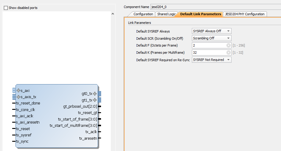
Here a screenshot of the Link parameters:

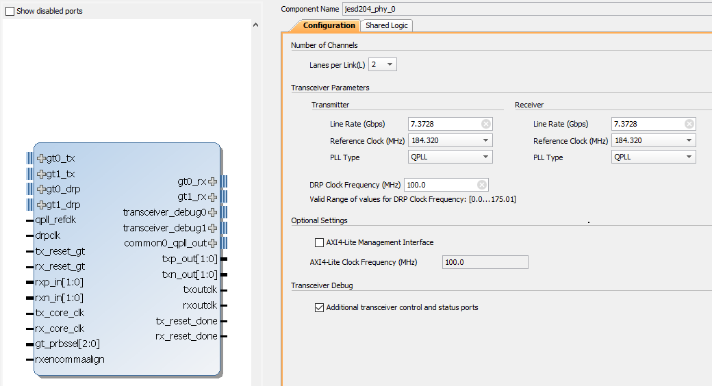
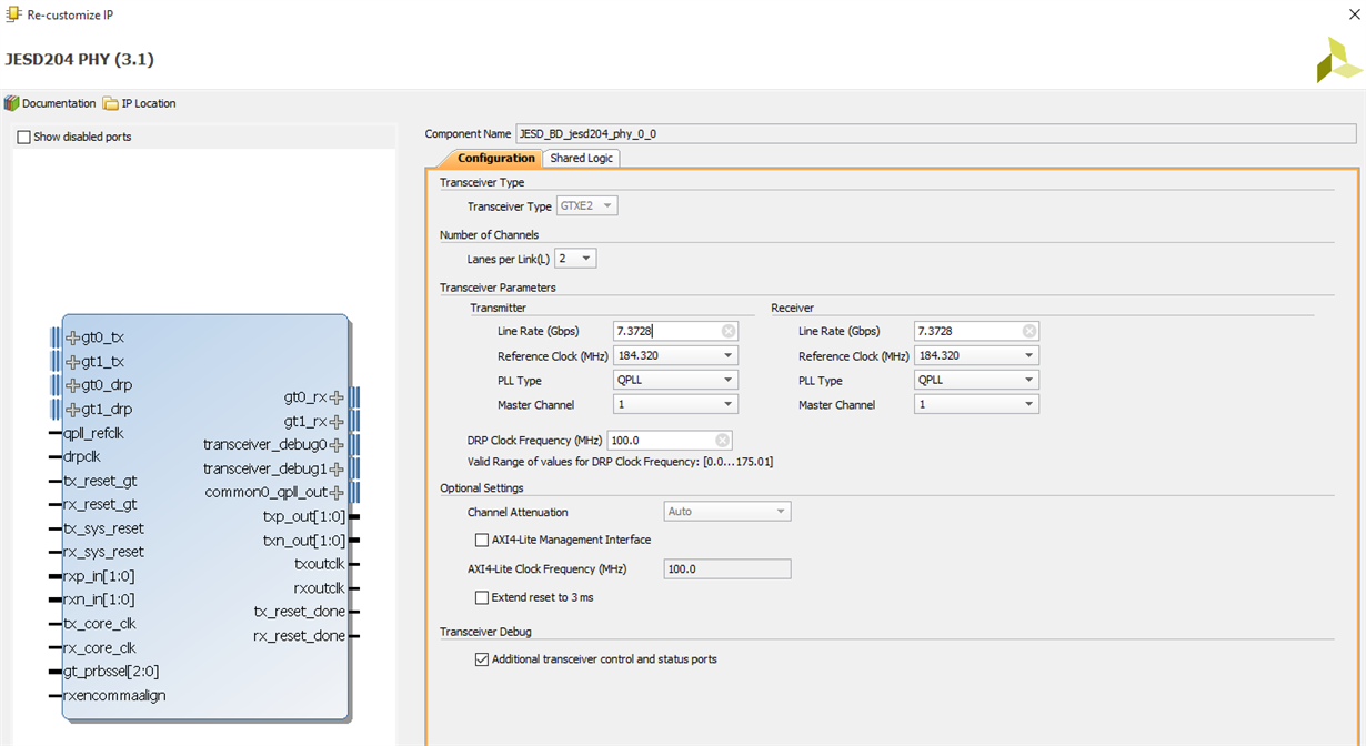
Here the screenshots of the JESD-PHY configuration:

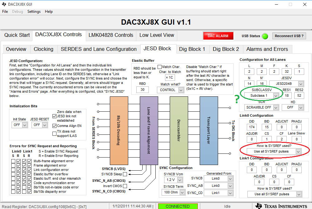
The DAC-configuration is as follows:

The JESD params are programmed with the same values as on the KC705:

See JESD-registers.txt, these are the JESD register settings on KC705:

5444.JESD-registers.txt
    --------------------------------------------
    -- config 0
    --
    -- Default set always used on reset - F = 1, K = 32, Scrambling OFF
    --
    0   => x"8008",    -- Addr x008             Rx Config 0                                   
    1   => x"0000",    -- Data x0000_0001       Enable Lane Alignment                         
    2   => x"0001",                                                                           
    
    3   => x"800C",    -- Addr x00C             Rx Config 0                                   
    4   => x"0000",    -- Data x0000_0000       [0] Disable Scrambling                        
    5   => x"0000",                                                                           

    6   => x"8020",    -- Addr x020                                                           
    7   => x"0000",    -- Data x0000_0000       [7:0] F (octets per frame) = 1                
    8   => x"0000",                                                                           

    9   => x"8024",    -- Addr x024                                                           
    10  => x"0000",    -- Data x0000_001F       [4:0] K (Frames per multi) = 32               
    11  => x"001F",                                                                           

    12  => x"8014",    -- Addr x014             Tx Only                                       
    13  => x"0000",    -- Data x0000_0003       [7:0] ILA multiframes = 4                     
    14  => x"0003",                                                                           

    15  => x"880C",    -- Addr x80C             Tx Only                                       
    16  => x"0000",    -- Data x0000_0FAE       [15:12] BID = xF  [7:0] DID = xAE             
    17  => x"0FAE",    --    
    
    18  => x"8810",    -- Addr x810                                              
    19  => x"0010",    -- Data x0010_1002       [25:24] CS=0 [20:16] N' = x10 [12:8] N = x10  [7:0] N = x2           
    20  => x"1002",    --                
    
    21  => x"8814",    -- Addr x814                                                 
    22  => x"0401",    -- Data x0401_0100       [28:24] CF   [16] HD [12:8] S                                   
    23  => x"0100",                                                                           

    24  => x"8818",    -- Addr x818             Tx Only                                       
    25  => x"0000",    -- Data x0000_1234       [7:0] RES1 [15:8] RES2                                    
    26  => x"1234",                                                                           

    27  => x"0000",    

See DAC37J82_Settings.cfg, these are the DAC register settings:

8168.DAC37J82Settings.cfg

The sine wave output on the analog lanes looks as follows:

DAC alarms are as follows:


It seems to be a synchronisation error, but I'm struggling with the reason how this can happen. Clocks to the FPGA REFCLK = 184.32 and Core clock = 92.12 are correct, FPGA is in SYNC. Is there a specific DAC startup-sequence in addition to RESET DAC JESD-Core and Trigger SYSREF ?

Please take a look to the DAC register config and JESD config: do you see any mismatch ?

In addition to this problem, we do not see any correct analog output using the http://www.ti.com/lit/zip/slac690 Xilinx firmware or downloading firmware to KC705 as described in SLAU580A and SLAU547B.

Please, could you send me a DAC37J82 config file which has the correct DAC settings to interconnect with the http://www.ti.com/lit/zip/slac690 Xilinx firmware.


Thanks in advance.

Regards,

Zoltan Gergely

  • Zoltan,

    None of your screen shots got through. Please send the DAC config file you are loading and the ini file you are using with HSDC Pro GUI. What application is this for?

    Regards,

    Jim

  • Hi Jim,

    Hopefully the attachment can be uploaded this time:

    3324.JESD-registers.txt
        --------------------------------------------
        -- config 0
        --
        -- Default set always used on reset - F = 1, K = 32, Scrambling OFF
        --
        0   => x"8008",    -- Addr x008                                              
        1   => x"0000",    -- Data x0000_0001       Enable Lane Alignment                         
        2   => x"0001",                                                                           
        
        3   => x"800C",    -- Addr x00C                                               
        4   => x"0000",    -- Data x0000_0000       [0] Disable Scrambling                        
        5   => x"0000",                                                                           
    
        6   => x"8020",    -- Addr x020                                                           
        7   => x"0000",    -- Data x0000_0000       [7:0] F (octets per frame) = 1                
        8   => x"0000",                                                                           
    
        9   => x"8024",    -- Addr x024                                                           
        10  => x"0000",    -- Data x0000_001F       [4:0] K (Frames per multi) = 32               
        11  => x"001F",                                                                           
    
        12  => x"8014",    -- Addr x014             Tx Only                                       
        13  => x"0000",    -- Data x0000_0003       [7:0] ILA multiframes = 4                     
        14  => x"0003",                                                                           
    
        15  => x"880C",    -- Addr x80C             Tx Only                                       
        16  => x"0000",    -- Data x0000_0FAE       [15:12] BID = xF  [7:0] DID = xAE             
        17  => x"0FAE",    --    
        
        18  => x"8810",    -- Addr x810                                              
        19  => x"020F",    -- Data x020F_0D01       [25:24] CS=2  [20:16] N' = xF  [12:8] N = xD  [7:0] M = 2           
        20  => x"0D01",    --                
        
        21  => x"8814",    -- Addr x814                                                 
        22  => x"0101",    -- Data x0101_0000       [28:24] CF=1   [16] HD=1  [12:8] S=1                                   
        23  => x"0000",                                                                           
    
        24  => x"8818",    -- Addr x818             Tx Only                                       
        25  => x"0000",    -- Data x0000_1234       [7:0] RES1 [15:8] RES2                                    
        26  => x"1234",                                                                           
    
        27  => x"0000",      

    TB_config.cfg

    All settings are related to the test bench configuration mentioned in Xilinx PG066 (JESD204 v6.2) document, chapter 6. Only paramter M is different. It's 2 in our case, means encoded value programmed is 1.

    Here the screenshots of the JESD configuration:

    The application is used for RF communication system.

    We're not using HSDC Pro GUI at the moment, only the DAC GUI. We're generating sine wave data in the FPGA application itself.

    Regards,

    Zoltan

  • HI all,

    I did not receive any reply on my former request yet, but I madesome progress on this issue.

    I modified the application on the KC705 to support 2 lanes instead of 4 and send sine wave data on 2 lanes:


    Please have a look to the JESD register settings in the KC705 FPGA application:

    jesd_configs.txt
       --------------------------------------------
        -- config 0
        --
        -- Default set always used on reset - F = 2, K = 32, Scrambling OFF
        --
        0   => x"8008",    -- Addr x008                                              
        1   => x"0000",    -- Data x0000_0001       Enable Lane Alignment                         
        2   => x"0001",                                                                           
        
        3   => x"800C",    -- Addr x00C                                               
        4   => x"0000",    -- Data x0000_0000       [0] Disable Scrambling                        
        5   => x"0000",                                                                           
    
        6   => x"8020",    -- Addr x020                                                           
        7   => x"0000",    -- Data x0000_0001       [7:0] F (octets per frame) = 2                
        8   => x"0001",                                                                           
    
        9   => x"8024",    -- Addr x024                                                           
        10  => x"0000",    -- Data x0000_001F       [4:0] K (Frames per multi) = 32               
        11  => x"001F",                                                                           
    
        12  => x"8014",    -- Addr x014             Tx Only                                       
        13  => x"0000",    -- Data x0000_0003       [7:0] ILA multiframes = 4                     
        14  => x"0003",                                                                           
    
        15  => x"880C",    -- Addr x80C             Tx Only                                       
        16  => x"0000",    -- Data x0000_0FAE       [15:12] BID = xF  [7:0] DID = xAE             
        17  => x"0FAE",    --    
        
        18  => x"8810",    -- Addr x810                                              
        19  => x"020F",    -- Data x020F_0D01       [25:24] CS=2  [20:16] N' = xF  [12:8] N = xD  [7:0] M = 2           
        20  => x"0D01",    --                
        
        21  => x"8814",    -- Addr x814                                                 
        22  => x"0100",    -- Data x0100_0000       [28:24] CF=1   [16] HD=0  [12:8] S=1                                   
        23  => x"0000",                                                                           
    
        24  => x"8818",    -- Addr x818             Tx Only                                       
        25  => x"0000",    -- Data x0000_1234       [7:0] RES1 [15:8] RES2                                    
        26  => x"1234",                                                                           
    
        27  => x"0000",                                     


    As you can see: octets per frame = 2 (programmed value is 1, as described in the datasheet).


    Please have a look to the DAC settings:

    2_lanes_interpolation_1_no_SYSREF.cfg

    As you can see: octets per frame = 2 (programmed value is 1, as described in the datasheet, register 0x4B = 0x1D01).

    With this settings, I see noisy sine wave data output on both DAC analog output lanes.

    If I reduce the number of octets per frame on the KC705 side, means octets per frame = 1 (programmed value is 0, as described in the datasheet), I can see sine wave data without any noise on both DAC analog output lanes.

    What could be the reason of such a behaviour ?

    Thanks in advance.
    Zoltan

  • Here the sine wave output signals.


    1. octets per frame = 2 (programmed value is 1, as described in the datasheet) on KC705 and DAC:

    2. octets per frame = 1 (programmed value is 0, as described in the datasheet) on KC705 and octets per frame = 2 (programmed value is 1, as described in the datasheet) on DAC:

  • Zoltan,

    When using a K =32, the SYSREF must be equal to 5.76MHz with the DAC clock at 368.64Msps. This is a divide by 512 when using the DAC GUI. When I went from a K=10 to K=32 with my setup, if I did not change the SYSREF divider, bad data occurs because SYSREF was shorter than LMFC period. The LMFC = Fs/(K*F) and max SYSREF = LMFC. SSYSREF can also be LMFC/n where n = 1,2,3...

    Regards,

    Jim 

  • Hi Jim,

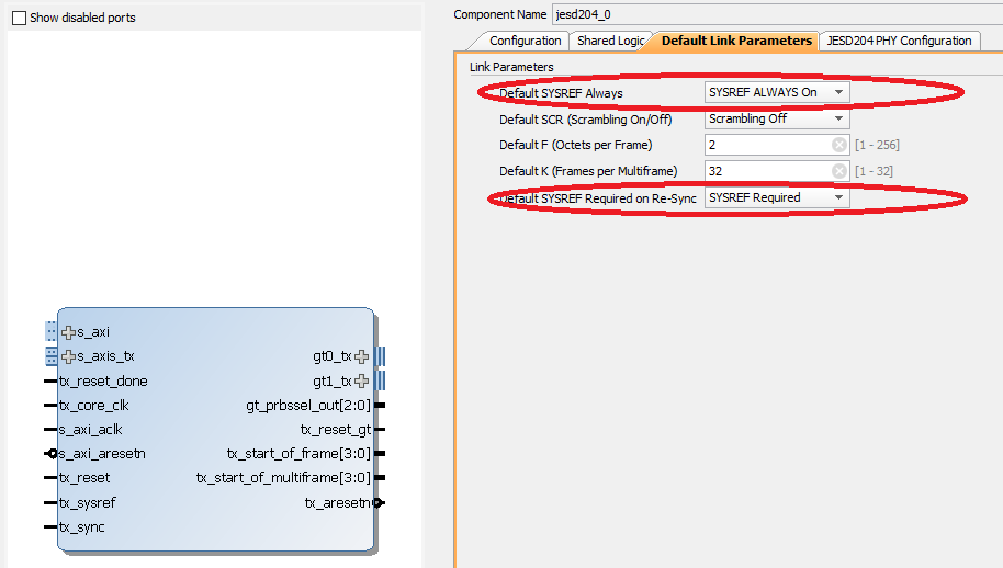
    We tried to use Subclass-0 mode, because it's the easiest mode to establish and to verify a link. See the screenshots of the JESD config above: SYSREF always off, SYSREF not required.

    By the way: the datasheet of the DAC says:

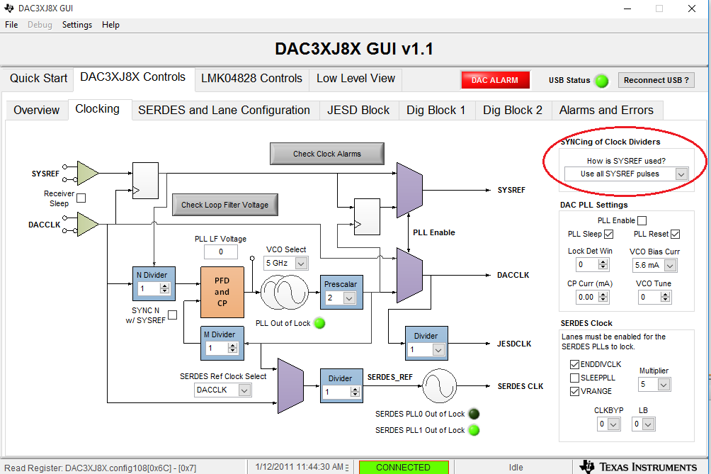
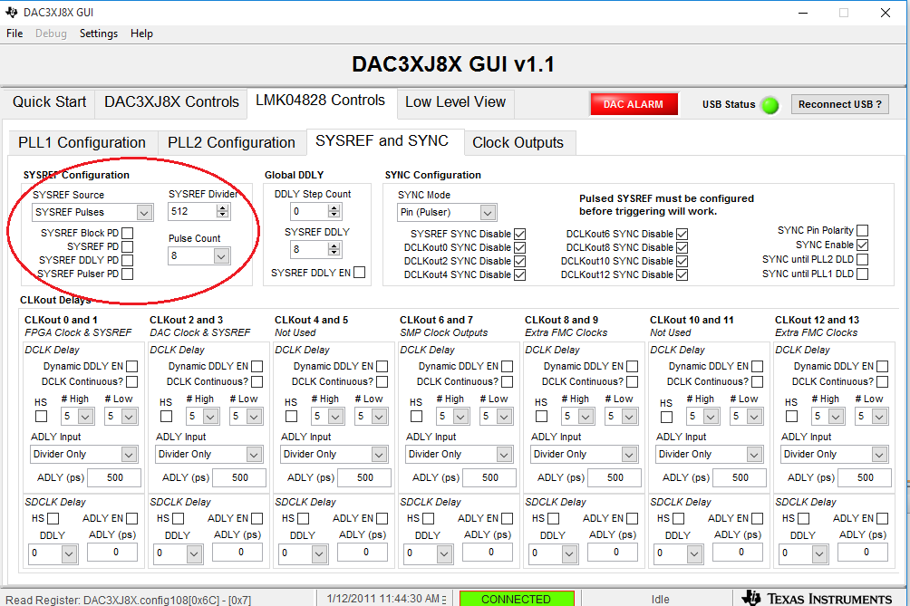
    Why is there still a possibility in the DAC GUI to set Subclass0 and Subclass2 mode as well? Here a screenshot, together with the new SYSREF config:


    And the other screenshots from the SYSREF config items on the DAC side:

    See the whole DAC config:

    2_lanes_interpolation_1_SYSREF_pulsed.cfg

    JESD config on the KC705 side to use SYSREF:

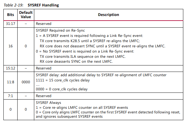
    SYSREF handling register contains the value 0x00010001:


    Unfortunately, the result is still the same:

    Noisy data if octets per frame = 2 (programmed value is 1, as described in the datasheet) on KC705 and DAC:


    Correct data if  octets per frame = 1 (programmed value is 0, as described in the datasheet) on KC705 and octets per frame = 2 (programmed value is 1, as described in the datasheet) on DAC:

    Did you encounter such an effect (means not the same "octet per frame" config on FPGA and DAC side) somewhen during your tests as well?

  • Another observation is the following:

    If I reset the JESD core on the KC705 (trigger tx_reset) and trigger SYSREF on the DAC, sometimes data on channel 1 is incorrect, sometimes data on channel 2 is incorrect, sometimes both channels are incorrect, sometimes both channels are correct:

    Synchronization after reset seems to fail.

    Could this be related to the "octet-per-frame" issue described above?

    Thanks in advance.

    Regards,

    Z.

  • Z,

    What version of JESD204B IP and Vivado are you using? There has been issues in the past like this with early versions of the IP. Are you showing any of this to Xilinx? They may be able to help you. What is the current value for K that you are using? What is the desired LMFS you need to operate at?

    Regards,

    Jim  

  • Hi Jim,


    First application was with Vivado 2015.2 and JESD IP Version 6.1 (Rev.2). Afterwards (2 weeks ago) I upgraded to Vivado 2016.1 and JESD IP Version 7.0 . Still the same issue!

    Investigation from Xilinx side is on progress.

    As you can see in the screenshot above: K=32

    LMFS = 2221

    Could you send me a valid/correct DAC configuration for my XILINX app desicribed in this post (see attached JESD/DAC config and DAC-GUI screenshots) ? This would help a lot to isolate possible config mismatches between Xilinx-JESD side and DAC side.

    Thanks in advance.

    Regards,

    Zoltan

  • HI all,


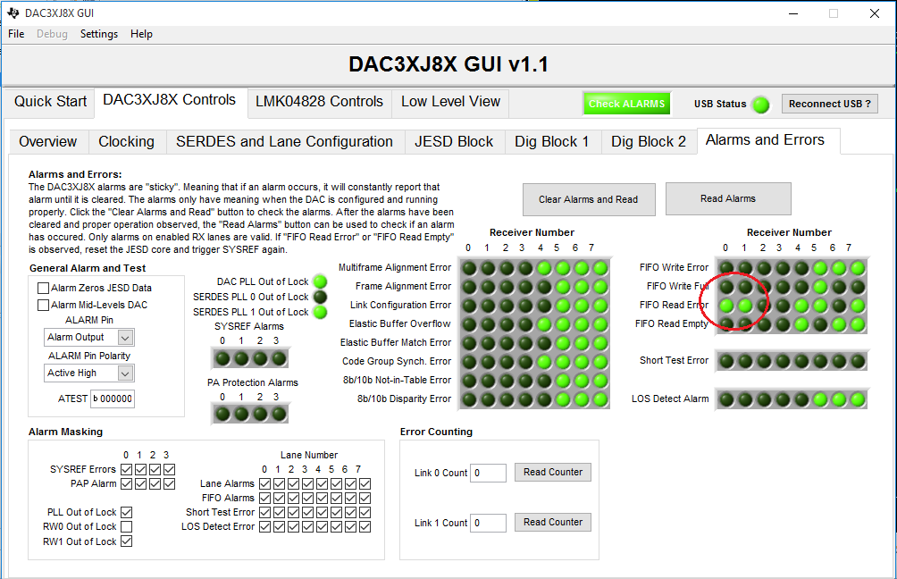
    After getting the correct sine wave output on the DAC side, I still get some FIFO read/write alarms:

    How can this happen (SYNC signal is stable, no resynchronization!) and whats the exact meaning of FIFO read/write alarms ?


    Datasheet says only:

    FIFO write error. Occurs if write request and FIFO is full.
    FIFO read error. Occurs if read request and FIFO is empty.

    Thanks in advance.

    Regards,

    Z.

  • Zoltan,

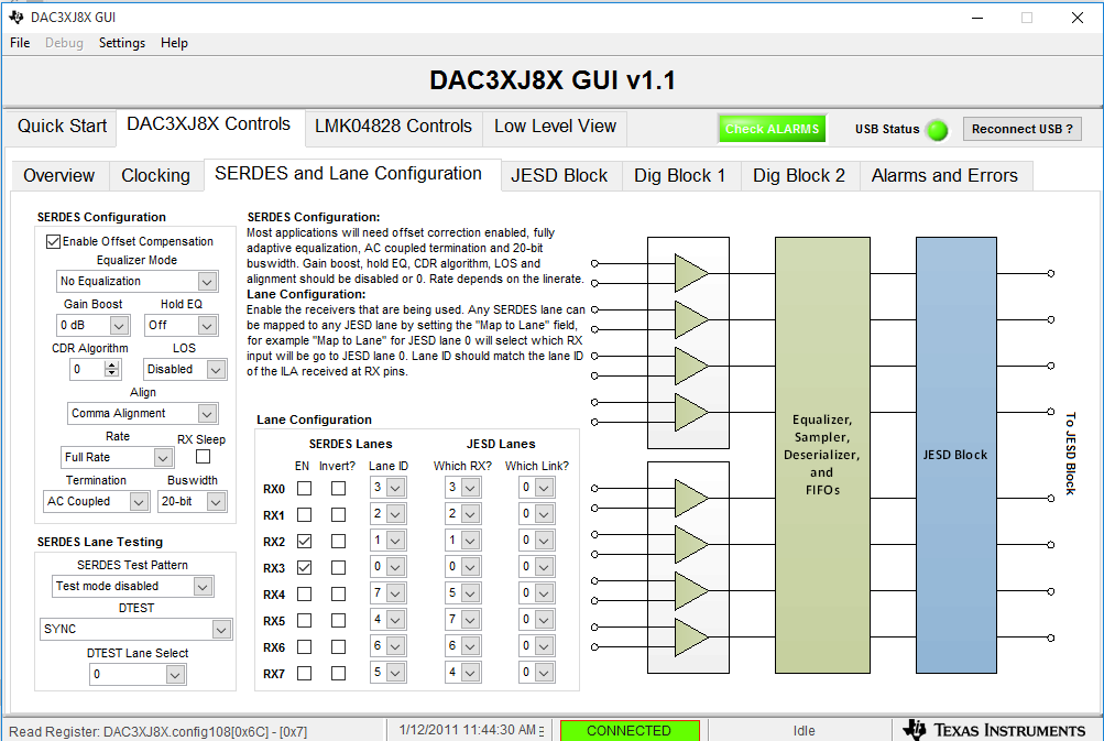
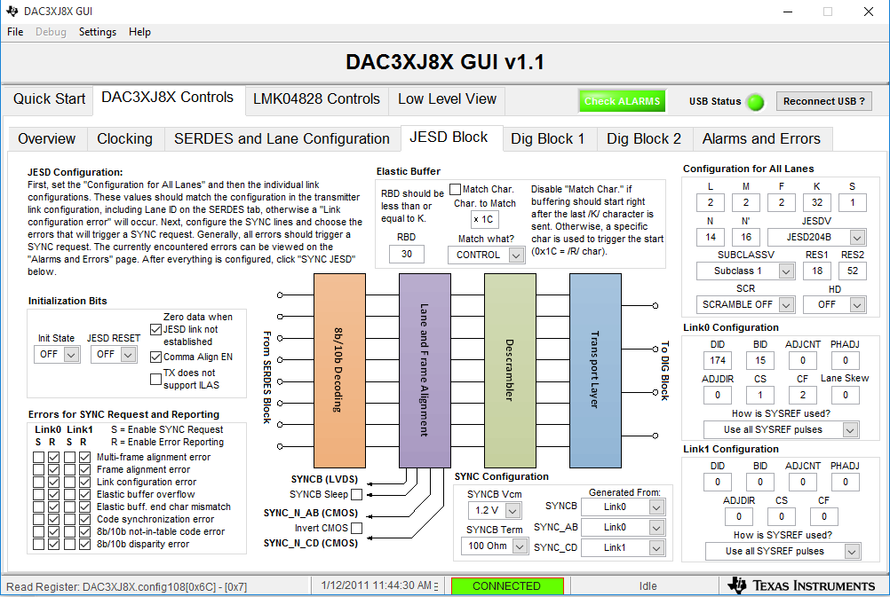
    What value of K are you now using? What is the SYSREF frequency? Can you send screen shots of the DAC Serdes and Lane Conf tab and the JESD Block tab?

    Regards,

    Jim

  • Hi Jim,


    Still the same config as before, but on the KC705 side I created some IP-Cores out of example design sources and interconnected them in a block design.

    Means K = 32 and as you suggested: When using a K =32, the SYSREF must be equal to 5.76MHz with the DAC clock at 368.64Msps. This is a divide by 512 when using the DAC GUI.

    See the screenshots below:

    An here the whole DAC config data:

    2843.2_lanes_interpolation_1_SYSREF_on.cfg

    What could be the reason for the FIFO alarms?

    Thanks in advance.

    Regards,

    Zoltan

  • Hi Jim,


    I did not receive any feedback from you yet.

    In the meantime a XILINX FAE was on site and we could do some detailed debugging, but the issue is still unsolved.

    Still the same settings as described in the former reply to your questions.

    Here some additiona lscreenshots:

    1. DAC config (config file attached in the former reply):

    2. XILINX JESD-PHY core config:

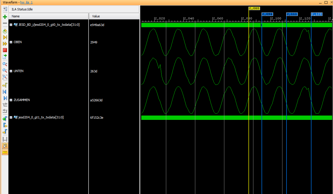
    3.The sine-wave that we saw on Vivado internal logic analyzer. It's the data sent from JESD-Core to JESD-PHY core:  Oben & Unten are the upper and the lower 14 bits, the Zusammen are the whole 28 Bits of data that we transmit over one transceiver:

    4. analog output zoomed out, the upper yellow line looks worse than the lower one, however the error is probably the same. The red signal shows somw sine-wave. The pattern can change between the upper and the lower channel or can be garbage on both:

    5. analog output zoomed in, you see the individual signal-levels on both channels with the same duration. However on the red channel you see the stepping better and also some hint of the sine-wave. The highest value decreases slightly over each “gap”, probably to the next ower values. The step-functions in between were the ones that I mentioned as “interleaved”:

    The issue is quite urgent, because design needs to be ready in a few days.

    Do you have any ideas what could be the reason for such a behavior ?

    Thanks in advance.

    Regards,

    Zoltan

  • Zoltan,

    Sorry about not getting back sooner. To many fires to fight. I will look at this first thing in the morning.

    Regards,

    Jim

  • Zoltan,

    See the attached file for our DAC setup. The KC705 used the following settings:

    JESD IP Core_CS=0
    JESD IP Core_F=2
    JESD IP Core_HD=0
    JESD IP Core_K=10
    JESD IP Core_L=2
    JESD IP Core_Lane_Enable=3
    JESD IP Core_M=2
    JESD IP Core_N=16
    JESD IP Core_NTotal=16
    JESD IP Core_S=1
    JESD IP Core_SCR=0
    JESD IP Core_LaneSync=1
    JESD IP Core_Subclass=1

    Regards,

    Jim

    DAC37J82_222_KC705.pptx

  • Hi Jim,

    Thanks for the reply.

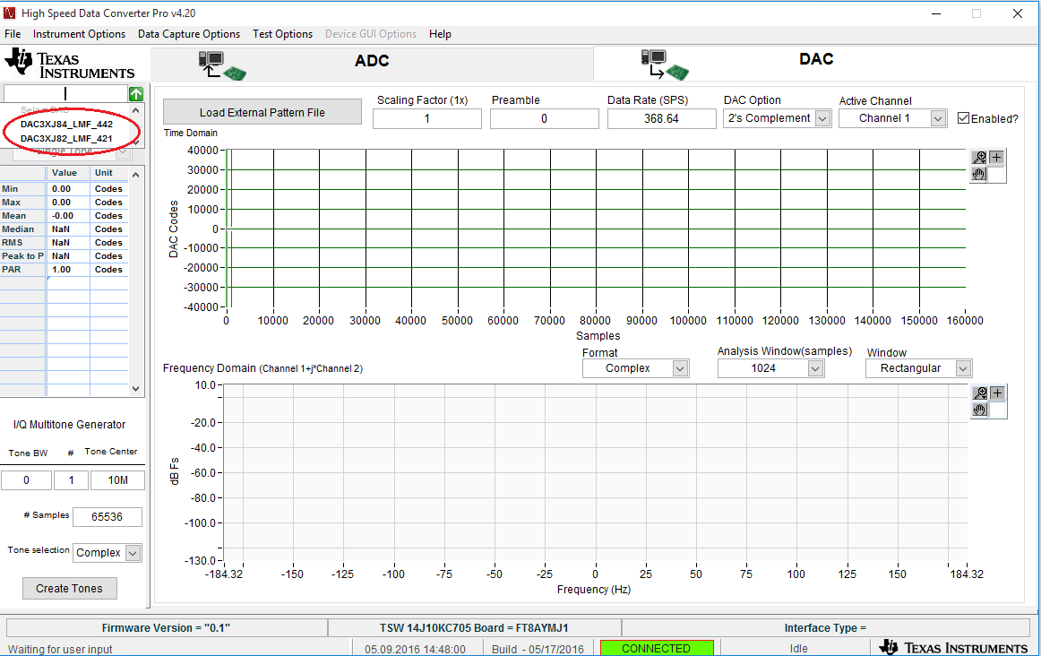
    Unfortunately, the HSDC GUI does not offer LMF_222 config:

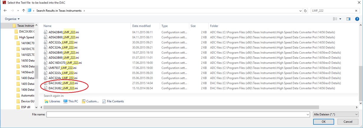
    But the .ini files for LMF_222 setting are present:


    What could be the reason why HSDC GUI does not offer LMF_222 selection ?

    Now whats really interesting in the JESD config you describe above is

    JESD IP Core_N=16
    JESD IP Core_NTotal=16

    This means 16bit data and no control bits. Our application is 14bit data and 2 control bits.

    DAC datasheet (SLASE16B) says:

    Last week, I was testing with a design where the JESD config was

    JESD IP Core_N=14
    JESD IP Core_NTotal=16
    JESD IP Core_CS=2

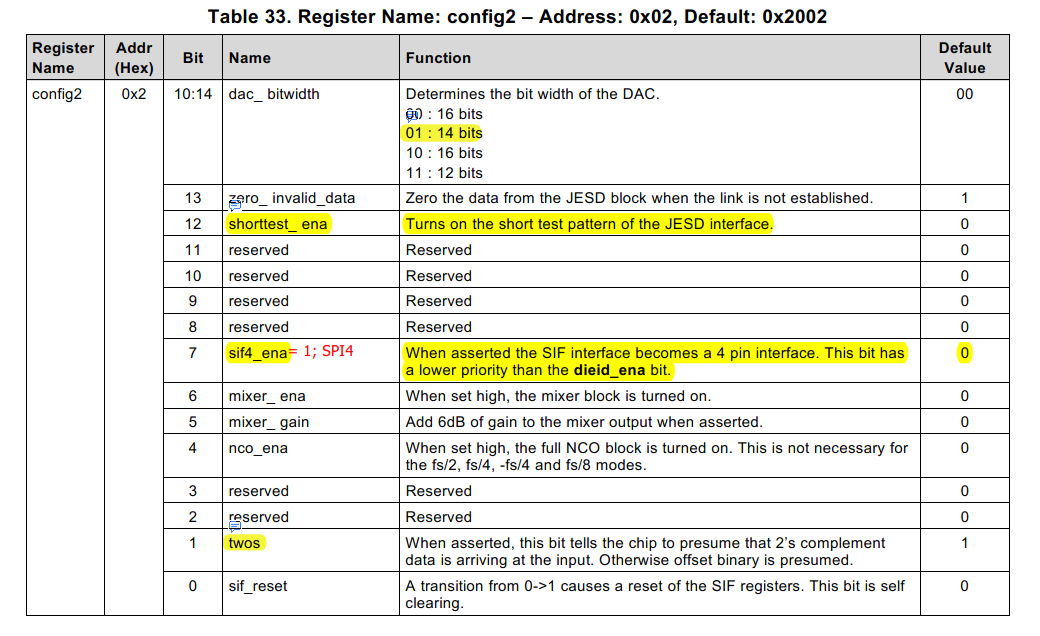
    When changing the bit settings for the "dac_bitwidth" (by the way: bit 10:14 seems to be a typo, it's 15:14, right ? ), it has absolutely no effect on the DAC output. Even after JESD-Core reset on DAC side.

    Today morning, I implemented a design which generates 16bit data and JESD config is like described in your design:

    JESD IP Core_N=16
    JESD IP Core_NTotal=16
    JESD IP Core_CS=0

    Sine wave on analog ouptuts looks good:

    But the same issue with this design: When changing the bit settings for the "dac_bitwidth" (by the way: bit 10:14 seems to be a typo, it's 15:14, right ? ), it has absolutely no effect on the DAC output. Even after JESD-Core reset on DAC side.
    Why this? Does the DAC37J82 support 14bit bitwidth or not? Or is this a bug inside the DAC?
    Another issue which is still present:

    If I reset only the JESD cores on the KC705 and do not reset the DAC JESD core (on the DAC EVM), I get quite often (approx. every 2nd  time) noisy data on one or both channels:

    zoomed:

    If I reset the DAC JESD core (on the DAC EVM), after that I reset the XILINX JESD-Core (on KC705), after that I trigger SYSREF on DAC à  the SYNC pin goes low, means device in SYNC but no data on DAC analog output --> I need to reset the reset the XILINX JESD-Core (on KC705) again and trigger SYSREF on DAC again --> I get only sometimes (approx. every 5-10th time)  noisy data on one or both channels.

    What could be the reason for this reset/resync issue ?

    Thanks in advance.

    Regards,

    Zoltan

  • Hi Jim,

    Another observation which I forgot to mention is, that it doesn't matter if data on both channels is a sine wave or noisy, the DAC alarms on both channels are always:

    Whats the exact meaning of this alarm an why does it occur?

    Datasheet just says: "FIFO read error. Occurs if read request and FIFO is empty." But when does it happen and why ?

    Thanks in advance.

    Regards,

    Zoltan

  • Zoltan,

    This error usually occurs if the DAC CLK and data rate are not set to the proper frequencies. The internal FIFO is either over flowing or empting causing wrong data to be sent to the internal DAC's. What is your data rate coming out of the KC705? What is the DAC CLK rate? What is the interpolation setting and LMF settings?

    Regards,

    Jim 

  • Zoltan,

    The ini files you showed are for the TSW14J56EVM, not the KC705. If you need this mode, I can look into creating an ini for the KC705. I am looking into the other issues you are having.

    Regards,

    Jim

  • HI Jim,

    Here some screenshots which contain the information you're asking:

    An in addition, the DAC config file for the actual configuration, which means 16-bit mode:

    2_lanes_interpolation_1_lane_01_16bit_no_equalization.cfg

    Please give me also feedback to the two open questions:

    1.When changing the bit settings for the "dac_bitwidth" (by the way: bit 10:14 seems to be a typo, it's 15:14, right ? ), it has absolutely no effect on the DAC output. Even after JESD-Core reset on DAC side. Why this? Does the DAC37J82 support 14bit bitwidth or not? Or is this a bug inside the DAC?

    2. SUBCLASS mode selection in DAC-GUI: see my post from 18. August, datasheet says for config72 register: "001 is subclass 1 and this is the only mode supported" but DAC GUI contains a selection box to configure Subclass-0 and Subclass-2 mode as well and bits will be set in config72 register. Which subclass modes are finally supported by DAC37J82?

    Thanks in advance.

    Regards,

    Zoltan

  • Zoltan,

    What is the end application for this?

    Regards,

    Jim

  • Zoltan,

    Can you change your reference clock to 368.64M and the LMK CLKout 0 and 1 divider to 8? This will match what my firmware is operating at. I also have K = 10.

    Regards,

    Jim

  • Hi Jim,

    I created a design on the KC705 to use 368.64MHz reference clock (instead of 184.32MHz) and set the CLKout 0 and 1 divider to 8.

    --> I've tested the new setup but still the same two issues:

    1. Resync after RESET fails approx. every 5th time (noisy data on one or both analog output channels)
    2. FIFO read error still persistent

    Do you have any other hints ?

    Thanks in advance.

    Regards,
    Zoltan
  • Hi Jim,

    In addition, I'm sending you the DAC revision number:

    DAC37J82I
    41ZCWQ9 G1

    Could it be a "first revision" device ?

    Regards,
    Zoltan
  • Zoltan,

    The revision of silicon you have is fine. Compile a new Xilinx project from the firmware that is under the TSW14J10EVM product folder and compare the parameters used by this project with yours.

    Regards,

    Jim 

  • Zoltan,

    Config2 register 0x02 sets the DAC output bits used for the analog generation, not the JESD204B input data to the DAC. You cannot change this to 14 bits and add 2 CS bits.

    Regards,

    Jim

  • Zoltan,

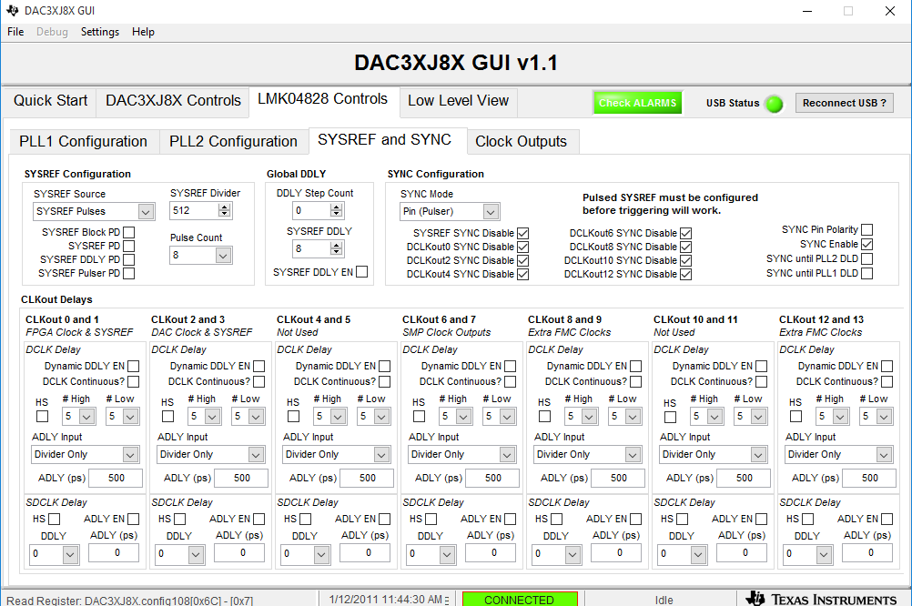
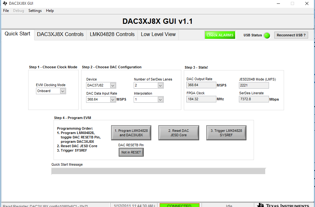
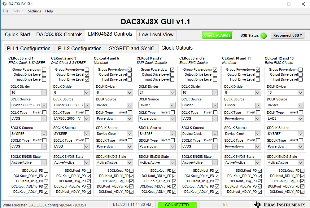
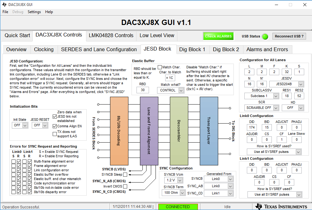
    I hear you are still having problems. Please explain your current status and send screen shots of the DAC GUI so I can try to help you. I am interested in the top level GUI screen shot, the LMK04828 output clocks screen shot, the JESD Block screen, and Alarm and Errors screen.

    Regards,

    Jim


  • HI Jim,

    Yes, unfortunately there are still 2 open issues:

    First issue: See the post in this forum from Sep 5, 2016 2:12 PM. Description starts after the sentence "Another issue which is still present:"

    From XILINX side I received the following reset procedure advice:

    - Program and reset our TX core (means XILINX JESD core)
    - Reset the DAC JESD core
    - Trigger SYSREF

    If I do so, the following could be observed:

    - Program and reset our TX core (means XILINX JESD core): Our observation: SYNC on DAC side still high, no data on analog outputs of DAC.
    - Reset the DAC JESD core: Our observation: SYNC on DAC side still high, no data on analog outputs of DAC.
    - Trigger SYSREF: Our observation: SYNC on DAC side goes low, no data on analog outputs of DAC.

    BUT: data on analog outputs of DAC available if I reset the JESD-TX Core on KC705 again and afterwards trigger SYSREF on DAC side again. Regarding XILINX, this is not a correct behavior.

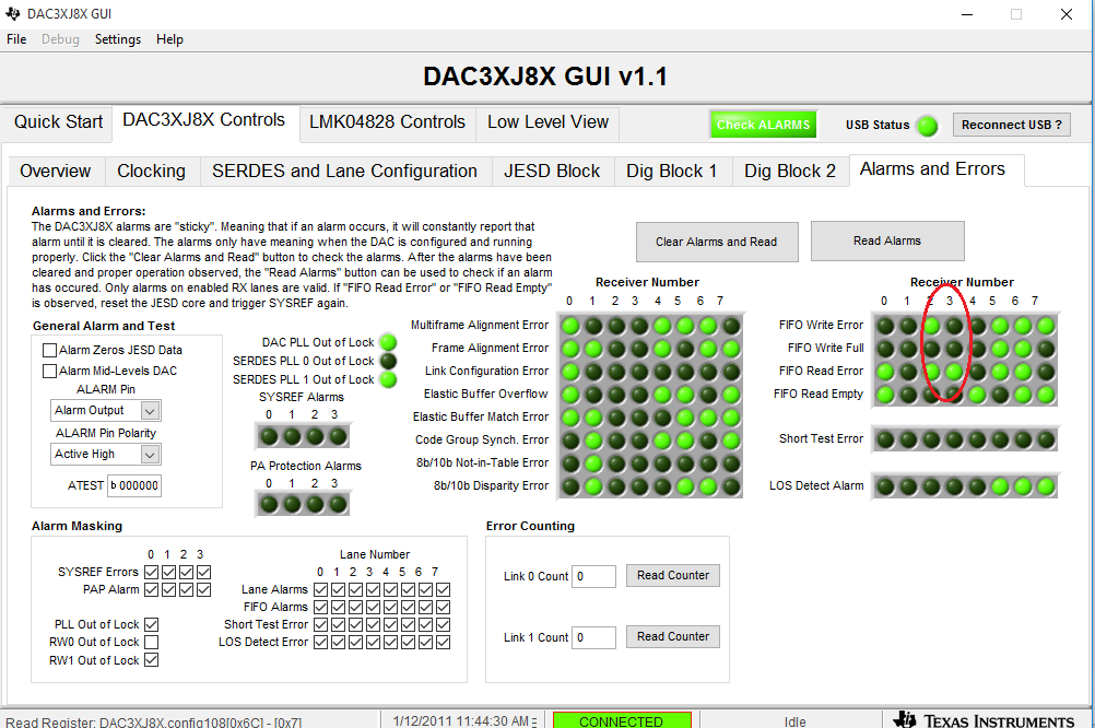
    Second issue: See the post in this forum from Sep 5, 2016 3:49 PM : FIFO Read Alarm always present, independent from the analog output: means even if sine wave correct on both analog channels, FIFO read error still present.

    Here now the requested attachments:

    Top-Level GUI:


    LMK04828 output:


    JESD Block(JESD params the same on Xilinx KC705):


    Alarm and Errors:


    In addition, the whole DAC config:

    5584.2_lanes_interpolation_1_lane_01_16bit_no_equalization.cfg

    Thanks in advance.


    Regards,

    Zoltan

  • Zoltan,

    The DAC is using lanes 2 and 3 so the FIFO read errors on lanes 0 and 1 can be ignored. CLK 0 &1 and CLK 12 & 13 cannot use the same divide value at this lane rate. CLK 12 & 13 divider should be twice of what CLK 0 & 1 are. Why do you have K = 32? What is your SYSREF divider set to?

    I am currently having trouble with this mode as well with my setup. I can get valid data from DAC A but not DAC B. The DAC synchronizes with no problems but the Xilinx firmware does not appear to be sending valid data on lane 1. I am checking with Xilinx regarding this. Make sure the clocks are present to the FPGA before loading firmware. After firmware is loaded, when I issue a DAC JESD reset and trigger SYSREF, I get valid data on DAC output A every time.

    Regards,

    Jim   

  • Hi Jim.

    Thanks for the reply.


    The replies step-by-step:

    The DAC is using lanes 2 and 3 so the FIFO read errors on lanes 0 and 1 can be ignored:  not for my design. I configured the .xdc file to send JESD TX-data to DAC input 0 and 1:

    # Place the GTXE2s
    set_property PACKAGE_PIN A3 [get_ports {txn[0]}]
    set_property PACKAGE_PIN A4 [get_ports {txp[0]}]

    set_property PACKAGE_PIN B1 [get_ports {txn[1]}]
    set_property PACKAGE_PIN B2 [get_ports {txp[1]}]

    CLK 0 &1 and CLK 12 & 13 cannot use the same divide value at this lane rate. CLK 12 & 13 divider should be twice of what CLK 0 & 1 are: according to SLAU580A, page 13 you're right:

    REFCLK = Lane rate / 10, and Core clock = Lane rate / 10 when lane rate is between 1G and 3.2G
    REFCLK = Lane rate / 20 and Core clock = Lane rate / 40 when lane rate is between 3.2G and 10.3G

    But the differecne of the analog output shows just a frequency devision:

    REFCLK = Core-CLK:

    REFCLK = 2xCore-CLK:

    Why do you have K = 32?  Yes: K=32

    What is your SYSREF divider set to?  512, as you suggested in one of your former replies.


    Now you say:

    After firmware is loaded, when I issue a DAC JESD reset and trigger SYSREF, I get valid data on DAC output A every time.

    But what happaneds if you reset XILINX-JESD core, reset DAC-JESD core and trigger sysref again.  Please do this minimum 10 times. Do you always get correct data on the DAC analog output lanes?

    In my setup, in 10-20% of the case I see noisy data on one or both analog channels.


    An the 2 other issues I mentioned are still present:

    1. Data on analog outputs of DAC available if I reset the JESD-TX Core on KC705 again and afterwards trigger SYSREF on DAC side again. Only one reset of DAC/Xilinx JESD core means no analog data on DAC output.

    2. FIFO Read errors always present

    Thanks in advance.

    Regards,

    Zoltan

  • Zoltan,

    When using the Xilinx generated firmware, if I set the core clk = ref clk, I get bad output data on CHA. The errors by the DAC in this mode  is attached. When I divide the core clk by 2, the data is good and I get no errors. I am assuming you are trying your own firmware, correct? I am still having issues with getting any data on CHB and working with our software team and Xilinx to try and figure out why this is. If I issue a FPGA core reset, then send data from HSDC Pro, then reset the DAC CORE and issue a SYSREF, I never get bad data out of CHA. I did this 20 times with no problems.

    Regards,

    Jim

    Presentation1.pptx

  • HI Jim,


    Thanks for the reply.

    I think the fastest way would be if I could send you my KC705 example design, because you already received the DAC config and with these two items you could reproduce the issues with my setup.

    Do you have Xilinx Vivado Studio installed ?

    If not, we should proceed with TSW14J10 (Info: we're not using TSW14J56 !) connected to KC705 and DAC-EVM. But the problem is as posted on Sep 5, 2016 2:12 PM . Unfortunately, the HSDC GUI does not offer LMF_222 config: Could you please generate and send me a HSDC GUI config for DAC 37J82 using LMF222 ? In addition the corresponding DAC config would help a lot.

    Thanks in advance.

    Regards

    Zoltan

  • Hi Jim,

    Thanks very much for the support, after I got a direct contact to a TI FAE, all problems are solved.

    The problems were:

    1.    Resynchronization (because sine generation and TX-DATA on KC705 side looks good) of the two JESD cores (KC705 and DAC side)  do you have any idea why the resynchronization could fail SOMETIMES or in another way: why we see noisy data on DAC output lanes ?
    2.    Reset-Issue: Why is data on analog lines only present if I reset the JESD core twice (!) and trigger SYSREF also twice (!), see description above ?
    3.    Why is FIFO_Read_Alarm always active (always means even if data correct on analog ouptuts, the DAC still sets these alarm bits)  ?

    Problem 1 + 2 solved:

    Solution: Clock settings should be:

    FPGA-Refclk = 368.64M (DCLK devider = 8)
    Core-Clk = 184.32M (DCLK devider = 16)

    In my design (where I encountered all 3 problems described above) the clocks were

    FPGA-Refclk = 184.32M  (DCLK devider = 16)
    Core-Clk = 92.16M (DCLK devider = 32)

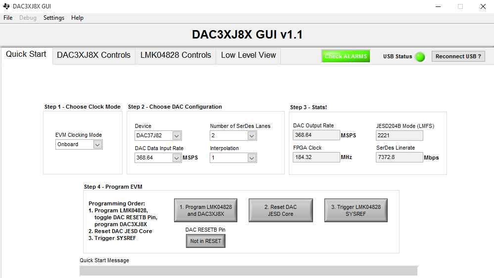
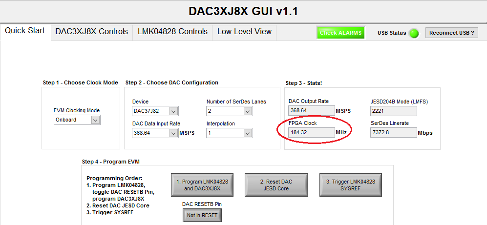
    So finally, the JESD-PHY REFCLK setting should be 368.64M instead of 184.32M . I took these clock frequencies because of the “FPGA Clock” value field in the DAC GUI.


    But for me it’s still not understandable why in 80%-90% of the cases the analog data was correct and only in 10-20% of the cases noisy data could be observed after resynchronization.Do you have a plausible explanation how this can happen ?


    Problem 3 solved:

    Solution: Solution of problem 1/ 2 as described above + Reset Xilinx JESD core AND reset DAC JESD core before triggering SYSREF.

    But if I do not reset DAC-JESD core after resting Xilinx JESD core, FIFO read alarm always occur, but data on analog line is correct.  Is this a correct behavior? Because DAC datasheet just says in chapter “Initialization Set Up” step 13. and 14. that DAC-JESD core should be reset before triggering SYSREF but there is no description in relation to the “external” Xilinx JESD core.

    Thanks in advance.

    Regards,
    Zoltan