This thread has been locked.

If you have a related question, please click the "Ask a related question" button in the top right corner. The newly created question will be automatically linked to this question.

ADS1248: measuring 4 Analog inputs and a single RTD

Part Number: ADS1248
Other Parts Discussed in Thread: INA159, INA826, OPA227, REF6025, ADS124S08, TPS65131-Q1

Hi,

I want to use a single ADS1248 for measuring 4 Analog inputs and a single RTD. The Analog inputs can be +/-10V or 4-20 m"a.

When measuring the voltage, the input need to be of high impedance (Cathode Protection)

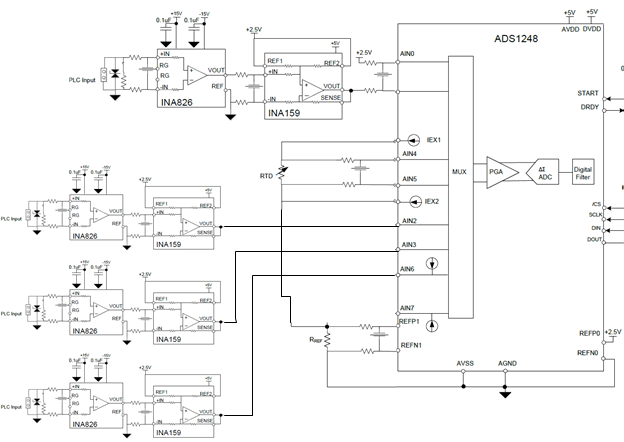
Following the tidu491 verified design guide can I use the following configuration?

Any other considerations?

Thanks

Noam Weodenfeld

  • Trying again to attach the picture

  • Noam,


    While I don't know TIDU491 design guide very well, it looks like you've just replicated the first channel three other times.

    In the first channel, it measures the PLC input through an INA826 and INA159 and measures it against +2.5V. I would note that you would do that for the other three channels as well. For the first duplicated channel, you'd select AIN2 as AINP and AIN0 as AINN, and use AIN0 for AINN for the other channels as well. I would also put in similar input filtering for the other channels.

    If you're measuring both ±10V and 4-20mA, I think that you'll need the current to be sunk by whatever you are using your 2.5V reference. Also note that any error that you have in the reference is an offset error for both the ±10V and 4-20mA measurements. You'll want that to be a precision reference.


    Joseph Wu

  • Joseph Hi,

    Thank you for the fast reply.

    There is a parallel resistor in every input channel that can be connected by a jumper for current measuring.

    I will add the filtering for the other inputs.

    Any suggestion for a voltage reference sources (2.5V and +/-15V)?

    Thanks

    Noam

  • Noam,


    For the ±2.5V reference, you could use the REF5025 or the new REF6025 which I haven't had a chance to use. I would note that neither can sink or source 20mA and you'd need to add a buffer of some sort. I'd use a low offset/low noise device like an OPA227 for that.

    As for ±15V, you'll need these for the INA supplies, but they don't need to be references. How you generate them depends on what voltage you start with. I'm not very familiar with products that you could use for these supplies and I'd ask this question in the power management forums (maybe starting with the Non-Isolated DC/DC forum).


    Joseph Wu
  • Joseph,

    I don't understand the current source/sink issue. The analog input is connected to a sensor which generates the current (Locally at the sensor) that run over the resistor at the INA826 inputs.

    Why do I need a current source for the 2.5V power?

    Noam
  • Noam,


    Sorry, I'd gotten it in my head that the current measurement would also be bipolar (based on another design I'd seen recently). In that case, you'd be sending the current to the +2.5V node and then measuring a test resistor going positive or negative for positive current and negative current. However, with the INA's, it wouldn't be a problem anyway.

    There are two other important things I'd like to point out:

    1. If you used a bipolar supply for the ADC, then you could use a simple resistor divider for the ±10V measurement. The ADC negative input would be connected to ground. In that case you'd be able to eliminate the INAs completely and you probably wouldn't need a ±15V supply.

    2. If you are willing to consider another device, then you should look at the ADS124S08. This new device is basically a next generation version of the ADS1248. It also has a 2.5V reference that you would be able to use in the measurement.


    Joseph Wu
  • Joseph Hi,

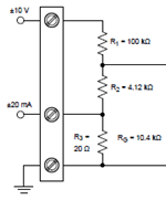
    You mean connecting a resistors net (Below) directly to the ADS1248?

    As I mentioned I need the input to be high impedance, that means that I need to use high value resistors for the resistors net. Wouldn't that be a problem?

    Noam

  • Noam,


    I thought I'd mention direct measurement of a resistor divider as a suggestion. I've seen it done in other systems.

    If you use high value resistors, then it might pose a problem. I generally don't like the resistance seen at an input to go above 10kΩ because it might disrupt sampling of the input. However, you could add a buffer to the output of the resistor divider if you want to keep high value resistors.

    Note that using the resistor divider requires that the supplies are bipolar. If the supply is unipolar (AVSS=0V and AVDD=3.3V or 5V) then AINN is set to ground in the measurement. Ground would be outside the input range of the PGA. In PGA=1, the input range goes from AVSS+0.1V to AVDD-0.1V.


    Joseph Wu
  • Joseph,

    So going back to the first configuration, INA826 and INA 159, this will be the best solution to buffer the input and keep the input impedance very high (The INA826 input impedance is measured in Giga OHM)?

    Also if I will change the ADC to ADS124S08 I can use its reference output as a common input for all Analog inputs i.e. connect the reference output to AINCOM?

    Noam
  • Noam,


    If you need input impedance into the GΩ level, then perhaps using the INA would be the best solution.

    I don't know what accuracy you'll need, but you should consider the error coming from the added offset and gain error from the two INAs. TIDU491 write up has a discussion about this in Circuit Performance Calculations section. It should cover the error contribution of the INA826 and INA159.

    If you do decide to use the ADS124S08, yes you'll be able to drive the INA reference pins to 2.5V with the REFOUT pin from the ADC. The reference will be able to sink and source 5mA, while the INA reference pins combined should use less than 1mA.


    Joseph Wu
  • Joseph,

    Can I use a boost switcher to generate the INA826 +15/-15V power e.g. TPS65131-Q1?

    Noam

  • Noam,


    I've never used the TPS65131-Q1 but it looks like it could handle the limited power of the devices shown in the schematic.

    We normally recommend that any switched power supply use an LDO before powering analog circuitry for a cleaner supply. Switching noise might degrade the ADC performance. The TPS64131 has been used in the past to directly power some of the SAR ADC devices (16-bit level). However, for the ADS1248 (24-bit level) you'll need a lower noise level for the resolution. Here's a link to a post with a brief description.

    e2e.ti.com/.../2106172


    Joseph Wu
  • Joseph Hi,

    Attached is the schematic for 4 Analog inputs (+/- 10V or 4-20 m"a) and a single RTD input. I hope the attachment process is OK.

    1. Can you let me know if the concept is OK.

    2. Regarding the input filtering, I used a single resistor (R610) and four capacitors for the analog inputs, is it OK or should I use a separate resistor for each input.

    3. The Maxim chip is a current limiter, I couldn't find something similar in TI. There is a bypass resistor if not needed.

    Thanks

    Noam

    Below is the file

    Analog Input.pdf


  • Noam,


    I don't see too many things to comment on, but I'll add a few things to think about.

    1. For the CLK pin, I would just ground it. It's probably ok floating it, but it is a digital input and it's hard to guarantee the state at start up.

    2. I would remove the ferrite bead from DVDD. I've seen cases where inductance on the digital supply will cause problems. With digital currents, you'll have large spikes of currents and with that LdI/dt, you may have problems with the supply spiking as well. It might not be a problem, but I would be prepared to bypass the ferrite if it does cause a problem.

    3. In general, we've done layouts with a single ground plane. It helps eliminate ground loop voltages between analog and digital ground. However, plenty of people do layouts with separate ground planes, just consider the return currents when working on the layout.

    4. I notices that yous some sort of transorb at the inputs for the RTD measurement. There are three DESD5V0S1BA-7 devices at the inputs. Note that any leakages between the reference resistor and the RTD will be seen as a gain error. Typically, the leakage current is 5nA, but over temperature this leakage may rise. The maximum is listed at 100nA. If this is ok as a error for you, then fine. Otherwise, you may need to find something with less leakage.


    Joseph Wu
  • Noam,


    There are two other things that I wanted to mention. First, I'm not too familiar with the MAX14626-S. It's a rather specialized function and I'm not sure if we have something similar. I'll look into it and if I find anything, I'll let you know.

    Second, at one point you mentioned that you wanted a high input impedance for the front end. I wanted to point out that the CDSOD323-T15SC has a maximum leakage of 1uA. In your application, I doubt that would be a problem, but I thought I would just point it out.


    Joseph Wu
  • Joseph Hi,

    One step before layout, I want to check with you some issues:

    1. Does the filters on the ADS1248 analog inputs are OK?

    2. What will happen when the analog input is not connected to the INA826 i.e. the "-" is connected to GND and the "+" is floating?

    3. Single GND layer or DGND and AGND connected with a ZERO OHM resistors?

    Thanks

    Noam

  • Noam,


    1. I think that's how you would set up the input filtering. I haven't seen a lot of single ended applications or X2Y capacitors used for input filtering. Normally, you would want the equivalent differential capacitance to be a factor of 10 larger than the common mode capacticance at each input so that any common mode signal coming in doesn't translate to a differential signal because of the capacitance mismatch. However, X2Y capacitors will likely have very good matching. In general, I'd have increased the differential capacitance, but you're probably ok.

    2. I'm not sure what will happen with a floating input for the INA826. I would post that question to the Precision Amplifiers Forum. The input impedance is rather high, and I would guess that it's possible for the input to float to any value. I wouldn't count on floating inputs to have a consistent behavior.

    3. Generally, we've recommended using a single ground plane for the layout. It helps eliminate ground loop voltages between analog and digital ground. However, plenty of people do layouts with separate ground planes, just consider the return currents when working on the layout.


    Joseph Wu
  • Joseph Hi,

    I have second thoughts about my design. Since the ADS1248 can sample one channel at a time there is no need to use 4 different channels for the analog signal sampling and voltage shifting (INA826 and INA159).

    I can multiplex the Analog input to the sampling circuit. By that I will reduce the HW and simpliphy the design and layout.

    Attached is the schematic, please let me know what you think of this architecture.

    Thanks

    Noam2746.analog input.pdf

  • Noam,


    In looking at the new schematic, I don't see too many changes other than the inclusion of a DG409 at the front end as an analog multiplexer. I don't think that there would be many problems with this. However, I'd had mentioned the leakage from the CDSOD323-T15SC in a previous post. With the DG409, your series resistance is typically 40Ω. This would react to the CDSOD323-T15SC leakage to give an error. This would represent a small error on your input signal which might vary with the input signal and temperature.

    Earlier, I hadn't looked at the input connection carefully because it was connected to the MAX14626-S. Now that I've had another look, I'm not sure I understand the INA826 connection. Shouldn't the -IN be to ground? Right now, it looks like you're measuring across the MAX14626-S. I'm assuming that your current sense measurement is either R656 or R597 protected by the MAX14626-S. That would also mean that you might need another jumper, since the +IN measurement of R597 should be after the MAX14626-S.


    Joseph Wu