This thread has been locked.

If you have a related question, please click the "Ask a related question" button in the top right corner. The newly created question will be automatically linked to this question.

ADS1278: ADS1278 sensitivity changes with sampling rate

Part Number: ADS1278
Other Parts Discussed in Thread: ADCPRO

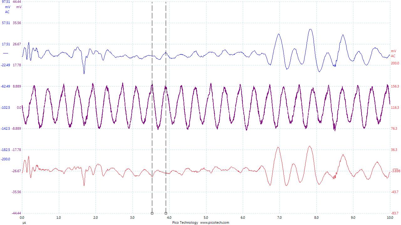
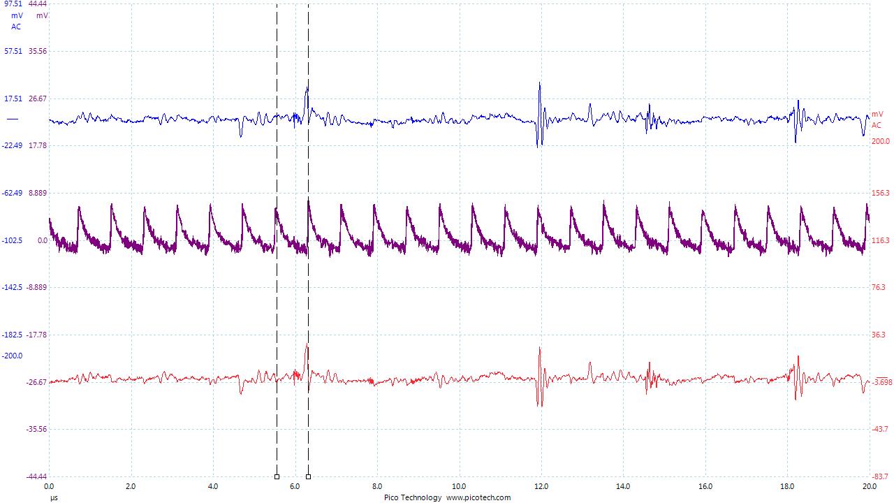
I am using the ADS1278 over a variety of sampling rates (1 ks to 30 ks).  When I change sampling rate it seems to change the sensitivity (Volts/count).  The change seems to be on the order of a few percent but doesn't seem to be monotonic with sampling rate (7 ks could be high, 8 low, 9 high again).  I am using it is high-precision mode.  Is this normal?  I would have thought that all of the sensitivities would have been within the tolerance of the 0.5% gain error on the data sheet.

  • Hello Joseph,

    Thanks for your post.

    The performance of the ADS1278 should not change all that much just by sweeping the output data rate (fDATA) from 1kSPS to 30kSPS. When you say the sensitivity changes, are you noticing a difference in noise performance? The volts/count (i.e. least-significant bit or LSB size) only depends on the reference voltage, the gain, and the ADC resolution. For a 2.5-V reference, the LSB size in the ADS1278 is 298nV.

    As you increase the sampling rate, the bandwidth of the digital filter does increase as well. The passband is defined as 0.453*fDATA. This allows a little more noise to appear at the ADC output. However, all acceptable data rates in High-Resolution Mode should meet the noise specifications in the Electrical Characteristics Table.

    Could you share more information about how you are collecting and analyzing the data? To compare the ADC noise alone, short the inputs of each channel to mid-supply and plot the data in a histogram format. From there, you can calculate the peak-to-peak and RMS noise. This should match the datasheet.

    Best Regards,
  • Thanks for the response.

    No I am not concerned with the noise.  I understand that that will change with sampling rate.  What I am seeing is a change in the sensitivity of the bits (what you quote as 298 NV per bit.  I am applying a fixed voltage (-1.8 VDC) with a 2.5 VDC reference and seeing the count change significantly (way more than the noise floor).  I have seen this both on the demo board using the TI provided software and on our production board via a microcontroller.  Below is some data I took on the demo board.  I have monitored both the input voltage and reference voltage with a DMM and scope as I change frequency and it does not change by more than ~0.1%.

    Clock Freq (MHz) Sample Rate (ks/s) Counts at 0 VDC Counts at -1.8 VDC
    0.5 1.0 -346.8 -6168319.4
    1 2.0 -158.3 -6162794.2
    2 3.9 -410.7 -6186670.5
    3 5.9 116.5 -6174868.4
    4 7.8 -139.0 -6168034.1
    5 9.8 -702.9 -6121254.7
    6 11.7 -99.3 -6171872.9
    7 13.7 -236.8 -6174944.0
    8 15.6 -280.9 -6177409.6
    9 17.6 -343.2 -6187448.8
    10 19.5 -885.0 -6258151.0
    15 29.3 -482.7 -6167600.6

      0385.1278 error graph.pdf

  • Hi Joseph,

    Thanks for sending the data.

    These devices are screened for the min/max Gain Error limits at final test, so I don't suspect this to be a device issue. In fact - the gain error should be much closer to the typical value rather than near the limits.

    I'd like to confirm a few details to make sure the measurement setup is correct:

    1. The gain error is specified in the datasheet with the offset error removed. I saw that you were measuring the offset, but wanted to confirm that you were subtracting it from the -1.8V measurement as well before computing the gain error. Then you can normalize it to the reference voltage to convert to %FS. Did you remove the offset error from the calculation?
    2. The offset voltage should be measured using an input-short condition. This is typically done by shorting the ADC inputs together directly at the pins and tying them to a min-supply common-mode voltage. Is this how you measured the offset? You can also short the inputs together elsewhere on the board (i.e. at the inputs of an amplifier), but you'll have to calibrate out the additional offset error in the signal path, per #3.
    3. Remember that if you use a DC source and/or include additional components in the signal path, the voltage at the ADC inputs will include the total offset of the signal chain. For both the 0V and -1.8V measurement, you should be measuring the voltage at the ADC inputs with a precision DMM and using that value as your input voltage.

    I would recommend taking the average of several samples at 0V and -1.8V for each data rate (perhaps focus on one at a time, as it should not vary). Then compute the gain error from those two averaged points.

    Best Regards,

  • Ryan,

    Yes, in my calculations I am subtracting out the offset error. The offset errors are generally small (< 0.1%) compared to the gain errors (~1%) but they are subtracted off by shorting the input pins anyway.

    All the data shown there is the average of 2048 samples as taken by the ADCPro software. I also have the standard deviations which are typically around 100 - 200 counts.

    Thanks,

    Joe
  • I have done some more testing and discovered that if I use the buffer amp on the demo board this problem goes away (<0.1% error across the sampling rate range). I have checked with a scope and the buffer amp effectively filters out the high frequency signal from the clock input. It seems likely that this means my error is coming from aliasing of this clock noise into the measurement. However when I measure this noise it is relatively constant with changing input voltage. Therefore I don't understand how this noise is causing a gain error. I can understand how it would cause an offset error but not a gain. I measured the error at several points and it is definitely a linear gain error.

    I have also tried on our board which has a very similar 10x gain amp with filtering and it does not fix this problem. Is there some other aspect to the buffer amp of the demo board that I am missing?

    Thanks,

    Joe
  • Hi Joe,

    One other possibility is that you are seeing the sampling transients produced by the switch-capacitor input stage of the ADC. These inputs are low-impedance and you'll notice a small voltage droop and recovery at the pins after each sample. These would occur at the modulator frequency, which is CLK / 4 for High-Resolution Mode. These transients will be much larger if you are probing at the ADC inputs and bypassing the amplifier. Or, if instead you probe the input voltage at the amplifier inputs, you should not see them at all. Were you measuring the input voltage in the same place and simply enabling/bypassing the amplifier?

    The settled voltage at the ADC inputs will change as you sweep the CLK frequency and this should be mostly linear. However, any overshoot and ringing can produce a non-linear error as well.

    Does this sound like what you might be seeing? Please send me some data and scope captures if you can so I better understand the issue.

    Thanks and regards,

  • Ryan,

    On the un buffered demo board there definitely are larger transients than with the buffer on.  It's possible this is what is causing the gain errors (the 1278 is sampling at a different point on the sine wave at different frequencies causing larger errors at those frequencies.  The transient values definitely increase at large Vins and the error is always within the magnitude of the transients.  With the buffer on there is still some transients however the waveform has areas when it goes to zero and perhaps the A2D is always sampling there.  Also note that at 5Mhz input frequency for some reason the ripple value on the unbuffered signal doubles.  I checked this several times and it always seems to happen at 5 MHz.  I did not see this at any other frequency.

    On my prototype board however the ripple is somewhere between the two but the error is larger than either.  On my board the error is well outside of the ripple value at some sampling rate.

    Below is a table of my measurements as well as a couple of scope traces.   To measure the ripple I had to subtract two single ended scope measurements so there is a bit more noise in the signal then I would like but it still seems to be an ok measurement.  The predicted VIn is based on the sensitivity at 1 Mhz between 0 and 1 Volt in.  my prototype board has a 10x buffer which is why the input voltages are different.  The voltage there is the voltage after the 10x buffer.

    Clock Buffer Modulator Sampling Vin Counts St Dev A-B PK-PK A-B Freq Predicted Vin Error (mV) Ratio
    1 N 0.25 2.0 0 -2820 46 1 0.000 0.00 0.00
    1 N 0.25 2.0 1.008 -3382033 47 10.5 0.25 1.008 0.00 0.00
    1 N 0.25 2.0 2.001 -6705893 62 19.15 0.25 1.999 1.51 0.08
    5 N 1.25 9.8 0 -3476 63 1 0.000 -0.20 -0.20
    5 N 1.25 9.8 1.008 -3360340 99 22 2.5 1.002 6.47 0.29
    5 N 1.25 9.8 2.001 -6663502 168 40.73 2.5 1.987 14.16 0.35
    8 N 2 15.6 0 -2786 54 1 0.000 0.01 0.01
    8 N 2 15.6 1.008 -3389879 48 9.6 2 1.010 -2.34 -0.24
    8 N 2 15.6 2.001 -6721467 48 15.89 2 2.004 -3.13 -0.20
    10 N 2.5 19.5 0 -3499 75 1 0.000 -0.20 -0.20
    10 N 2.5 19.5 1.008 -3431457 155 35 2.5 1.023 -14.74 -0.42
    10 N 2.5 19.5 2.001 -6804280 289 63.42 2.5 2.029 -27.84 -0.44
    20 N 5 39.1 0 -2707 40 1 0.000 0.03 0.03
    20 N 5 39.1 1.008 -3384132 34 9.7 5 1.009 -0.63 -0.06
    20 N 5 39.1 2.001 -6709847 39 12.24 5 2.001 0.33 0.03
    1 Y 0.25 2.0 0 -2253 38 1 0.000 0.00 0.00
    1 Y 0.25 2.0 1.008 -3378716 35 6.9 0.25 1.008 0.00 0.00
    1 Y 0.25 2.0 2.001 -6699624 32 11.89 0.25 1.999 1.58 0.13
    5 Y 1.25 9.8 0 -2250 40 1 0.000 0.00 0.00
    5 Y 1.25 9.8 1.008 -3379729 37 7.2 1.25 1.008 -0.30 -0.04
    5 Y 1.25 9.8 2.001 -6701471 181 11.3 1.25 2.000 1.03 0.09
    8 Y 2 15.6 0 -2234 41 1 0.000 0.01 0.01
    8 Y 2 15.6 1.008 -3379152 39 8 2 1.008 -0.13 -0.02
    8 Y 2 15.6 2.001 -6700387 35 11.26 2 2.000 1.36 0.12
    10 Y 2.5 19.5 0 -2338 40 1 0.000 -0.03 -0.03
    10 Y 2.5 19.5 1.008 -3378902 40 7 2.5 1.008 -0.06 -0.01
    10 Y 2.5 19.5 2.001 -6699846 35 11.8 2.5 1.999 1.52 0.13
    20 Y 5 39.1 0 -2133 35 1 0.000 0.04 0.04
    20 Y 5 39.1 1.008 -3377593 37 7 5 1.008 0.34 0.05
    20 Y 5 39.1 2.001 -6697445 41 10.1 5 1.999 2.24 0.22
    Clock (MHz) Buffer Modulator Sampling Vin Counts St Dev A-B PK-PK A-B Freq Predicted Vin Error (mV) Ratio
    0.51 Proto 0.13 1 0.0218 75879 1 0.022 0.00 0.00
    0.51 Proto 0.13 1 0.926 3134729 13.5 0.125 0.926 0.00 0.00
    0.51 Proto 0.13 1 1.803 6106716   26 0.125 1.805 1.52 0.06
    2.51 Proto 0.63 4.9 0.0218 75817 1 0.022 -0.02 -0.02
    2.51 Proto 0.63 4.9 0.928 3140131 12.37 0.625 0.928 -0.40 -0.03
    2.51 Proto 0.63 4.9 1.803 6118583 19.2 0.625 1.808 5.03 0.26
    3.99 Proto 1.00 7.8 0.0218 74729 1 0.021 -0.34 -0.34
    3.99 Proto 1.00 7.8 0.928 3061111 14.79 1 0.904 -23.76 -1.61
    3.99 Proto 1.00 7.8 1.803 5961113 20.6 1 1.761 -41.52 -2.02
    4.99 Proto 1.25 9.75 0.0218 77655 1 0.022 0.52 0.52
    4.99 Proto 1.25 9.75 0.928 3215743 12.74 1.233 0.950 21.95 1.72
    4.99 Proto 1.25 9.75 1.803 6266759 21 1.233 1.852 48.83 2.33
    7.68 Proto 1.92 15 0.0218 74050 1 0.021 -0.54 -0.54
    7.68 Proto 1.92 15 0.928 3053769 15.78 2 0.902 -25.93 -1.64
    7.68 Proto 1.92 15 1.803 5946497 20.61 2 1.757 -45.84 -2.22

    5MHz Input No Buffer  1 Volt in


    5MHz Input No Buffer  2 Volt in


    5MHz Input Buffer  2 Volt in

    5 MHz Proto Board 1.8 Volt in

  • Hi Joseph,

    Very nice job with the scope measurements. I myself have struggled with making similar measurements that were clean and conclusive.

    The input buffer is absolutely needed to settle the input voltage between samples. I'm assuming the purple curve in the middle of each plot is the differential voltage at the ADC inputs (i.e. the difference between the curves above and below)? Without the input buffer, I believe you are seeing the inputs oscillating (this is still a DC input voltage, correct? :) )

    The two plots with the input buffer at the bottom look closer to what I would expect to see. The input voltage settling is following the R-C time constant at the buffer output. Although the voltage does not flatten and fully settle, it should reach the same point after each sample for a given sampling frequency and DC input voltage, resulting only in a gain error. The gain error measurements will not be valid if the inputs to the ADC are ringing as shown in the first two images.

    Also, I noticed that the modulator frequency is only 625kHz in the last image taken from your proto board. Can you confirm that you are using the same ADC configuration?

    Best regards,

  • Ryan,

    Yes, the purple curve is the difference. I think I figured out what my problem was. The input buffer on the individual channels was working well but I did not have a sufficient buffer on the reference input. Because the reference input changes impedance so much with sampling rate I couldn't put the same kind of RC filter on it. I improved the buffer on my board and it is working well now.

    BTW the reason that the bottom image was sampled at 625 kHz was due to a error in my code which was giving me the wrong sampling clock.

    Thanks for your help.

    Joe
  • Hi Joe,

    I'm glad that you found the issue. I agree that an inadequate reference buffer can also produce a large gain error. Generally, we try to put a large capacitor at the output of the reference driver with proper compensation to maintain stability without any resistance in series with the reference pin. Smaller caps directly across ADC reference pins can help a lot with minimizing reference gain error as well.

    If you ever need us to review the supporting circuitry around the ADS1278, we would be happy to review your schematics in the future.

    Best regards,