Hi all,
I'm trying to use the Xilinx JESD204B transmitter IP core to send data to a DAC39J82 on our board. I'm having problems getting a healthy link established. I'll try to describe my problem first, and then I'll go over how I'm trying to setup the JESD link.
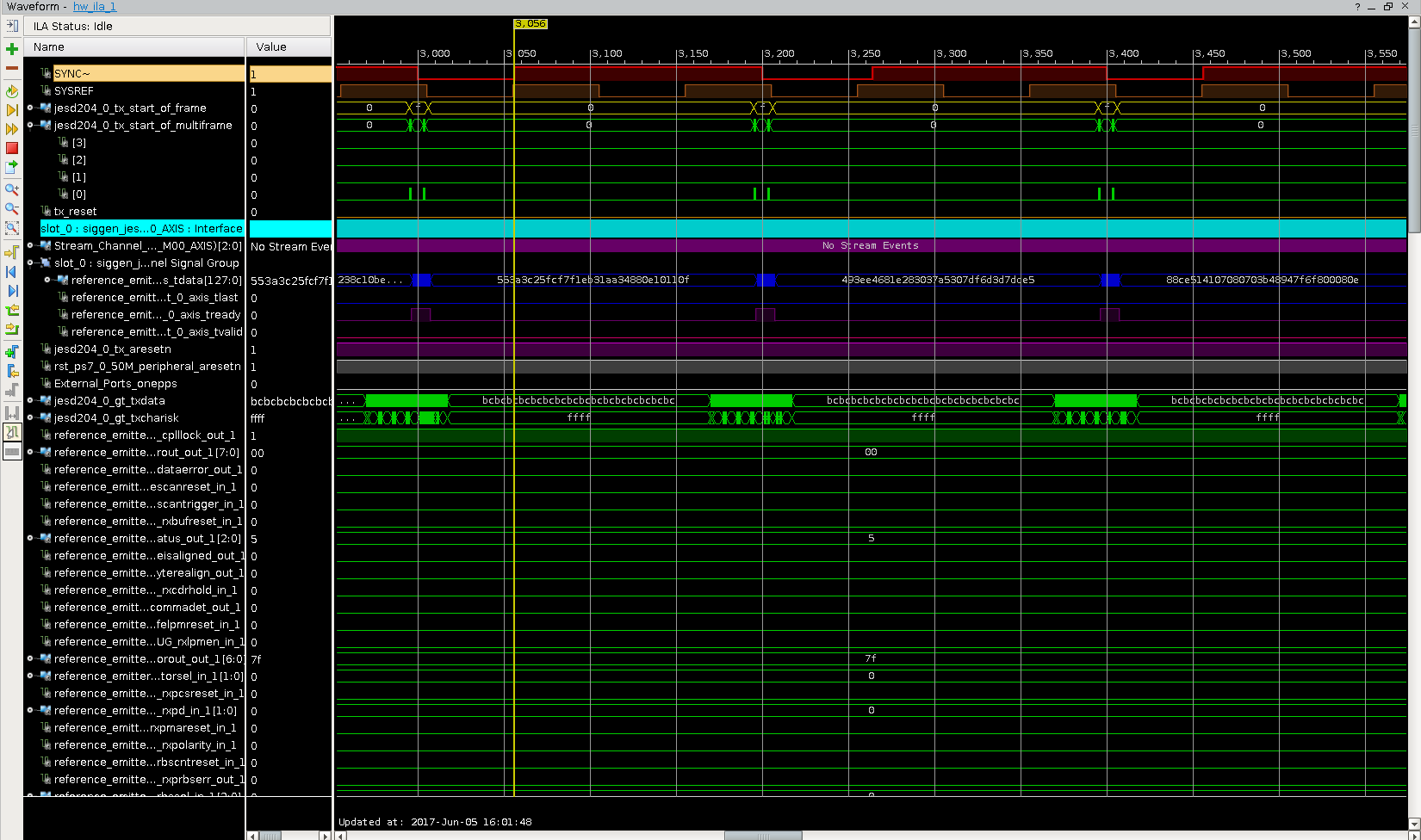
When bringing up the link I believe my system is failing to achieve ILA. I have both the JESD FPGA core and DAC initialized, and my SYSYREF signal set as a continuous periodic pulse. The SYNC~ from the DAC goes low, indicating that we are trying to resync. It then goes high, which I thought only happens after code group synchronization is achieved. The core then tried to put out some data and the DAC almost immediately drives the SYNC~ low again, trying to resync. This continues in a loop, and I have a waveform capture of the process from a logic analyzer core in my FPGA at the bottom of this post. The DAC lane alarm registers (config100 - 107) are indicating that my 4 lanes in use are all getting the "code synchronization error" and "8b/10b disparity error" bits set. These are defined in the actual JESD JEDEC standard sec 7.6.1 table 18 as "The state machine for code group synchronization has returned to the CS_INIT state" and "The received code group exists in the 8B/10B decoding table, but is not found in the proper column according to the current running disparity." respectively.
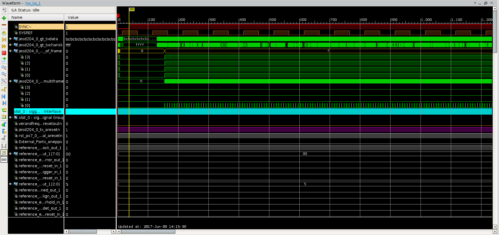
If you look at the included screencap you see that my JESD transmitter core is properly sending out the K28.5 commas (0xBC on txdata line) when SYNC~ goes low... so if I'm getting a disparity error I think that means the data is possibly getting corrupted en route to the DAC, or in the DAC itself. I am looking for advice on next steps to take to try to resolve my ILA issues. I feel like using the various test sequences is probably the answer, and I've tried, but I think I'm missing something in the setup because the TESTFAIL pin always just reads 0 (passing test), even when I intentionally feed in an incorrect sequence. I've tried using the PRBS 7 sequence and the continuous K28.5 character sequence.
My JESD setup is as follows: LMK is set to 421, 32 frames per multiframe, HD = 1, S = 1, elastic buffer = 31, serdes line rate is 6.25 Gbps total throughput, so 1.5625 GHz lane speed. My clocking is using a 1.25 GHz input at DACCLKp/n, I'm bypassing the DAC PLL and dividing down by 4 prior so that the serdes PLL reference clock is 312.5 MHz. This then is multiplied by 5 internally, and my serdes PLL output is then 1.5625 GHz. Register config108 is reading 0x07, indicating that serdes block 0 PLL is locking, block 1 is out of lock (expected since I'm only using the 4 lanes for block 0) and the DAC PLL is out of lock (expected since I'm bypassing it.) My JESD clock is set to be the DACCLK divided down by 8, so 156.25 MHz. My serdes is configured with ENOC = 1, fully adaptive EQ, CDR = 0, full rate, AC coupled termination, 20 bit bus width, gain boost = 0, LOS disabled and hold EQ off. I'll attach a print out of all my register settings as read from SPI (ie not sure alarms and such will be right because I literally am just reading all the registers in a loop.)
Sorry this post turned into a bit of a knowledge dump, but I don't know exactly what details you'll need to know to help me. Any advice? What additional info can I try to provide for clarification? I'm also talking to Xilinx support via email, but I'm more confident in the transmitter at this point due to there being fewer moving parts (less rope to hang myself with), and clearer documentation for that IP core than what TI provides for the DAC.
config0  : 0x118
config1  : 0x3
config2  : 0x82
config3  : 0xA301
config4  : 0xFFFF
config5  : 0xFFFF
config6  : 0xFFFF
config7  : 0x3500
config8  : 0x0
config9  : 0x0
config10 : 0x0
config11 : 0x0
config12 : 0x400
config13 : 0x400
config14 : 0x400
config15 : 0x400
config16 : 0x0
config17 : 0x0
config18 : 0x0
config19 : 0x0
config20 : 0x0
config21 : 0x0
config22 : 0x0
config23 : 0x0
config24 : 0x0
config25 : 0x0
config26 : 0x20
config27 : 0x300
config28 : 0x0
config29 : 0x0
config30 : 0x9191
config31 : 0x9180
config32 : 0x8008
config33 : 0x0
config34 : 0x1B11
config35 : 0xFFFF
config36 : 0x30
config37 : 0x6000
config38 : 0x0
config39 : 0x0
config40 : 0x3
config41 : 0xFFFF
config42 : 0x0
config43 : 0x0
config44 : 0x0
config45 : 0x1
config46 : 0xFFFF
config47 : 0x4
config48 : 0x0
config49 : 0x1000
config50 : 0x0
config51 : 0x0
config52 : 0x0
config53 : 0x0
config54 : 0x0
config55 : 0x0
config56 : 0x0
config57 : 0x0
config58 : 0x0
config59 : 0x1800
config60 : 0x228
config61 : 0x88
config62 : 0x108
config63 : 0x0
config64 : 0x0
config65 : 0x0
config66 : 0x0
config67 : 0x0
config68 : 0x0
config69 : 0x0
config70 : 0x44
config71 : 0x190A
config72 : 0x31C3
config73 : 0x0
config74 : 0xF01
config75 : 0x1E00
config76 : 0x1F03
config77 : 0x100
config78 : 0xF4F
config79 : 0x1CC1
config80 : 0x0
config81 : 0xFF
config82 : 0xFF
config83 : 0x0
config84 : 0xFF
config85 : 0xFF
config86 : 0x0
config87 : 0xFF
config88 : 0xFF
config89 : 0x0
config90 : 0xFF
config91 : 0xFF
config92 : 0x5
config93 : 0x0
config94 : 0x0
config95 : 0x123
config96 : 0x4567
config97 : 0x111
config98 : 0x0
config99 : 0x0
config100: 0x50A
config101: 0x50A
config102: 0x50A
config103: 0x50A
config104: 0xEC05
config105: 0xFB0F
config106: 0xEF0C
config107: 0x7F0E
config108: 0x7
config109: 0xF0
config110: 0x0
config111: 0x0
config112: 0x0
config113: 0x0
config114: 0x0
config115: 0x0
config116: 0x0
config117: 0x0
config118: 0x0
config119: 0x0
config120: 0x0
config121: 0x0
config122: 0x0
config123: 0x0
config124: 0x0
config125: 0x0
config126: 0x0
config127: 0x800A