This thread has been locked.

If you have a related question, please click the "Ask a related question" button in the top right corner. The newly created question will be automatically linked to this question.

DAC8563: Configuration for bipolar output

Part Number: DAC8563
Other Parts Discussed in Thread: REF5025, ADS8568

Hello, 

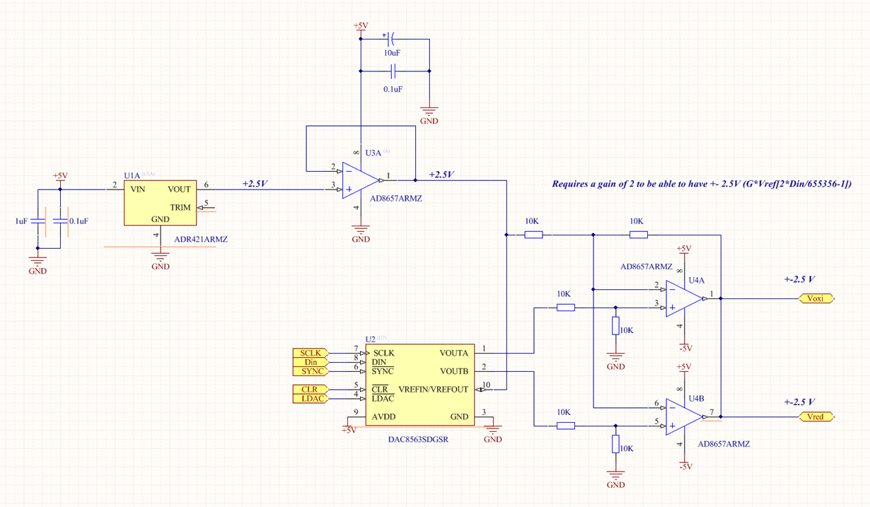
I am interested in using DAC8563 for my project. I want to be able to get +-2.5 V bipolar output for both of the output channels of DAC5863 with +2.5V external reference voltage. Although ithe bipolar output configuration is stated in the datasheet, the explanation is still unclear for me. As far as what I understand from the datasheet the following configuration should be implemented:

However I am not entirely sure if this is the correct one (or I would come up with an easier one).

Also if there is any C/C++ code for DAC8563, could you please help me to obtain that?

Thanks in advance,

Handenur Caliskan

  • Hi Handenur,

    Welcome to E2E and thank you for your query. In your circuit you are shorting the output of both the opamps. It will not work. Please refer to the following TI design for more details about the unipolar to bipolar conversion.

    www.ti.com/.../slau525.pdf

    You can also look at the EVM schematics: www.ti.com/.../sbau183a.pdf

    We currently don't have any C/C++ code. However, the SPI codes should be simple enough to program. If you are facing a problem in writing an SPI perpheral program, please contact the respective microcontroller team.

    Please let us know if you have any problems with register settings etc. We will be able to help you out with that.

    Regards,
    Uttam Sahu
    Applications Engineer, Precision DACs
  • Hello Uttam,

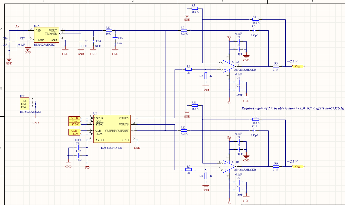
    Thank you for your help. I updated the circuit based on the design examples that you provide, I hope the +-2.5 V output will be achieved now. Furthermore, I want from the system to be as precise as possible. I added a low pass filter to the REF5025 around 3.3kHz (with R = 0.1K & C= 0.48µF) according to my signal of interest. However I am not sure whether a buffer is needed after filtering. So how should I decide that?

    I'd like to add a microcontroller which has at least 3 SPI + 1 SD card interface and a 16-24 bit 4-channel bipolar input of +-2.5V ADC to this circuit. ADS8568 seems interesting to me however it has 8 channels. Do you have 4-channel version similar to ADS8568 architecture? And any other recommendation for the µC and ADC to use in high sampling and precise biomedical instrumentation?

    Any help would be appreciated.

    Thank you.

  • Hi Handenur,

    You wouldn't generally need a buffer to drive the reference pin of DAC8563 as it has a constant input impedance. However, as the DAC and the op-amps in your circuit are going to draw current from the reference source. Further the current drawn by the op-amps will be code-dependent. The 10K series resistor at the reference output will then have a code-dependent voltage drop. Hence, it is a good idea to use an buffer after the filter. Please make sure that the bias current of the buffer is low enough to have any voltage drop across the 10K resistor.

    Regarding the ADC selection, could you please put a separate query? The ADC team should be able to answer it better?

    Regards,
    Uttam
  • Hi Uttam,

    Thank you for the answer.

    I have one more question, the datasheet says that the maximum voltage of the input high logic level can be AVdd and the minimum can be 0.7*AVdd. I want to set AVdd for +5V since I want to get +-5V for the analog output. Then the logic level in this configuration has a range of +3.5V to 5V. However, the microcontroller that DAC will be interfacing has a logic high voltage level of 3.3V. So there is a mismatch and actually it doesn't really make sense to get an input from a controller which has +3.5V at least. How can I solve this problem?

    If I decrease my AVdd to a lower value (which allows me to send a 3.3 V signal from the microcontroller to DAC) , will I be able to obtain +5V analog output from the DAC?

    Any help would be appreciated,
    Thank you.
  • Hi Handenur,

    You are facing a typical problem very common with single-power supply devices. Some of our new devices hence, have a separate IOVDD.

    However, now that you have chosen this device, there are different ways to solve the problem:

    1. The cleanest way is to use a level translator to convert between 3.3V from uC to 5V on DAC. There are many small size low-cost ICs available for this in TI
    2. Many new generation microcontrollers come with the output configuration as open-drain. If you are not planning to operate the device at very high speed and power is not a big constraint at the same time, you can use pull-ups to 5V on the SPI pins. Please make sure the pins are 5V tolerant before using this option. Many of the devices have this option
    3. The third option is that as you are using op-amp stages at the output, you actually don't need the DAC output to reach 5V. You can always change the gain settings such that the final output is in your required range irrespective of AVDD of DAC. You need to set the AVDD at around 4V to 4.5V in order to get a good tolerance on the Voh of the uC SPI signals.

    Regards,
    Uttam
  • Hi Uttam,

    Thank you for the answer. I would probably go with the third option.

    Best,

    Handenur