This thread has been locked.

If you have a related question, please click the "Ask a related question" button in the top right corner. The newly created question will be automatically linked to this question.

ADS54J60EVM: Inconsistent setup behaviour

Part Number: ADS54J60EVM
Other Parts Discussed in Thread: LMK04828

I have attached the ADS54J60EVM board to a Xilinx KCU105 developement board.The desire is to use an external 1GHz clock connected to J6. We want to run the JESD interface in 8224 format in subclass 1.

The Xilinx JESD core is setup to match the 8224 with K set to 16. I believe the line rate will be 5Gbps per second which means the core clock needs to be 125MHz. The core is configured to drive the core clock with the reference clock. Because of this I have modified the LMK04828 setup file to set the divider on the FPGA clock to 8. 

I then run the 8224 setup script for the ADC but tend to get varying results. I am using an ILA to monitor the lane outputs from the JESD_phy. Sometimes I get just zeros others what looks like valid samples but the sync signal is still low the core is not happy. I have used the ADS54Jxx GUI to force a resync and can get the BC pattern to appear although not always on all lanes. I have very occasionally got the sync to go high but not in a repeatable manor.  

As an aside the ADC occasionally becomes unresponsive, I am no longer able to change things via the GUI. This effects both the main page or ticking individual register bits.

I've read through some other forum but nothing seems to quite cover the issues i'm seeing.

Regards

Richard Hooper 

  • Hi Richard,

    I just looped in our apps engineer, and you should hear back soon.

    best regards,
    -Steve Wilson
  • Cheers, a few moments ago I did have it in a state that looked like it was sync'd at working but haven't managed to recreate it. The standard behaviour seems to be; the sync line from the FPGA is low but the ADC is throwing out what looks like samples on the lanes rather than sync/alignment characters and therefore nothing appears on the rx_tdata bus at the output of the core.
  • Richard,

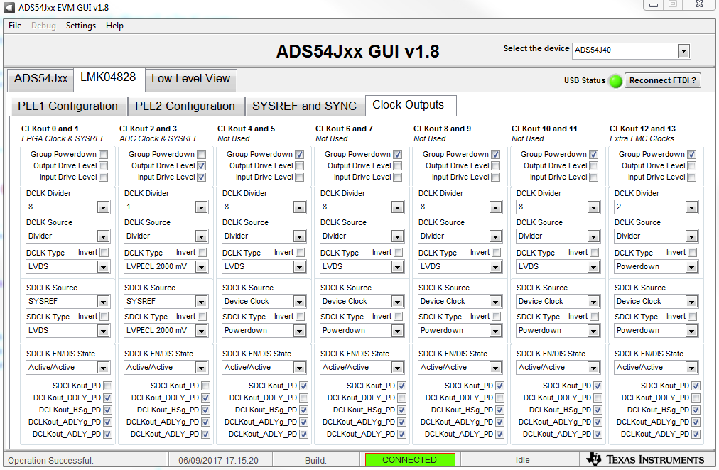
    If you are sending an external 1GHz clock to the LMK, you must use the LMK device in external clock mode. Can you send screen shots of the LMK output clocks and sysref and sync tabs? There are certain settings that must be set and I think you may have one of these wrong.

    Regards,

    Jim

  • For the case where I'm using the refClk to drive the core (125MHz). The SYSREF is setup to be 3.125MHz. 

    I have also tried reconfiguring the Xilinx core to use separate ref and glbl clocks. For this I change the clkout 0 divide to 4 to drive refclk with 250MHz and enable clkout8 with a divider of 8 to provide the glbl clock. 

  • Richard,

    When dividing by 1 with the DCLK in the LMK tab, you must set the DCLK Divider to "Divider+DCC+HS". Other wise the output is unstable. In our example when using a very similar setup (see attached), we provide a core clock that is the ADC sample rate/4 (250MHz in your case) to the KCU105. You may want to try this as well.

    Regards,

    Jim

    7823.KCU105 HSDC Pro User's Guide.pdf

  • The literature for the Xilinx JESD204 core (pg066) is very clear that the core clk should be 1/40 of line rate. I'm pretty sure that for our 8224 setup the line rate is 5Gbps so the core clock should be 125MHz. The refClk (that powers the GT tiles) could be 250MHz and as i've stated I have tried this method but not had any stable results either.

    Have you any idea why the ADC becomes unresponsive. Sometimes i'm able to use the GUI to do software SYNC or force an ILA pattern but then other times none of the writes seem to take and read backs of already set registers come back with zeros so it's very hard to confirm what settings the ADC is using in this state.
  • Richard,

    The configuration files that come with the TI ADC and DAC EVM GUIs are setup to operate with the

    Altera-based TI TSW14J56EVM. These files will work with the TSW14J10EVM when using a Xilinx

    platform but need a couple of changes to the settings of the LMK04828 registers. The firmware for the

    Xilinx Development Platforms use a separate clock input for REFCLK and Core clock to give maximum

    flexibility and support all line rates and subclasses with a single programmable design. The Xilinx IP used

    in the firmware can be driven by a single clock in many circumstances (see the clocking section of the

    Xilinx IP product guide for more details).

    The REFCLK and Core clock are determined by the following lane rate conditions:

    REFCLK = Lane rate / 10, and Core clock = Lane rate / 10 when lane rate is between 1 G and 3.2 G

    REFCLK = Lane rate / 20 and Core clock = Lane rate / 40 when lane rate is between 3.2 G and

    10.3125 G.  This is why our system uses the core clock setting I mentioned and yours is different..

    The GUI buttons are unstable and I would suggest not using them. Stick with the provided configuration files, create your own configuration files, or use the low level register read write option only. Are you issuing the board reset after the sample clock is up and running? How much current is your power supply able to provide to the EVM? Make sure this is at least 3A. Did you change the DCLK divider setting like I mentioned in the last post? Did this help?

    Regards,

    Jim 

  • Sorry for the delay in replying, I got it into a working state this morning and didn't want to fiddle with things whilst I was looking at some other aspects.

    I have switched to using a 250MHz refclk with 150MHz glbl (core) clock. Therefore I enable CLKout12 on the LMK. I had also switched the DCLK source. I have just power cycled everything and using these setting do seem to be able to achieve sync again although I do have to reprogram the FPGA. In our real design the FPGA will have access to the SPI lines for the ADC and LMK but for some reason you don't pass these down the FMC connector on your eval board. I'll have a play with holding the core in reset until i've set up the clocks via the GUI and hope that gives me consistent results.

    One of the aspects that I was trying to workout when I had data flowing from the ADCs was the ordering of the samples on the rx_tdata bus. The results we were getting are not what we would have expected. I realize this may be something we need to raise with Xilinx but given the way the samples were grouped per lane seemed to be unexpected means the transmitter (ADC) could also be doing something weird. I believe it is all setup for subclass 1 mode. I have the SYSREFClk permanently running to the device and FPGA at 3.125MHz. K is set to 16 which I believe makes our LMFC clock 15.625MHz.

    Dividing the 256bit rx_tdata bus in to 16 bit sections (starting with the LSB) the following mapping gives the true sample order. Within the 16bits the bytes had to be swapped but looking at the way the octets are packed I think this is to be expected.

    sampleA0 = section4
    sampleA1 = section6
    sampleA2 = section2
    sampleA3 = section0
    sampleA4 = section5
    sampleA5 = section7
    sampleA6 = section3
    sampleA7 = section1
    sampleB0 = section12
    sampleB1 = section14
    sampleB2 = section10
    sampleB3 = section8
    sampleB4 = section13
    sampleB5 = section15
    sampleB6 = section11
    sampleB7 = section9

    Does this mean that some frame and or lane alignment isn't working although it seems to be consistent across power cycles. It's hard to find a fully drawn out example for an 8224 setup so if you have one available that might help.
  • Richard,

    Do you still have questions regarding this?

    Regards,

    Jim 

  • No one seems to have answered my last question about which samples are appearing in which lanes

  • Richard,

    The Xilinx firmware we use with the TSW14J10EVM processes samples from Lane 0 to Lane 7, using the JESD204B VITA FMC spec to determine which FMC pins correspond to which lanes. Since the ADS54J60EVM did not route these lanes 1:1 to optimize the routing, the data is processed in a different order, as shown by the attached file. Hope this helps.

    Regards,

    Jim

    8224 lane mapping.docx

  • That helps a lot. I'm surprised with the octet ordering on the final mapping. My experience is that the MSB byte is put on the bus first assuming you're filling up the rx_tdata bus from the LSB.