This thread has been locked.

If you have a related question, please click the "Ask a related question" button in the top right corner. The newly created question will be automatically linked to this question.

TSW4806EVM: TSW4806EVM Frequency Issue

Part Number: TSW4806EVM

I have a customer having issues in getting the TSW4806EVM to produce a 100MHz clock. Here is the explanation that he gave:

I am doing everything I can to get the module generate a 300MHz and 100MHz clock using TSW4806 EVM board.
Instead, I got 303MHz and 101MHz, respectively and each clock has a fairly large jitter that varies from 298MHZ to 305MHz as a min. and max. repetitive rate.

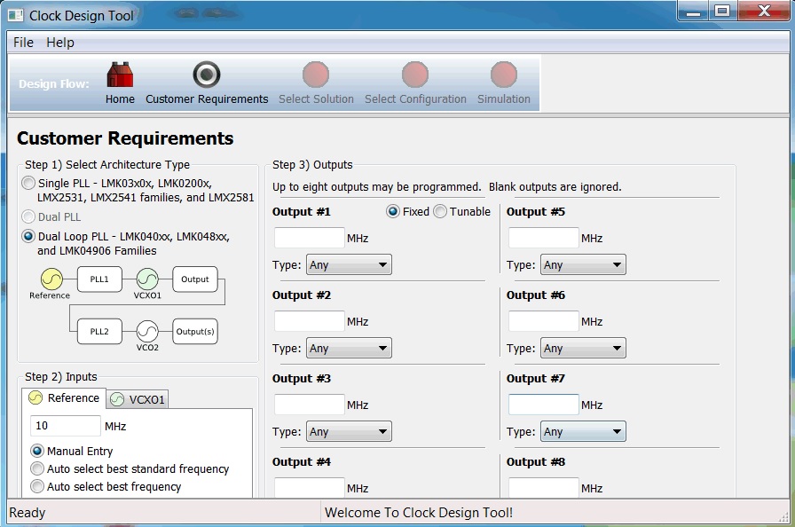
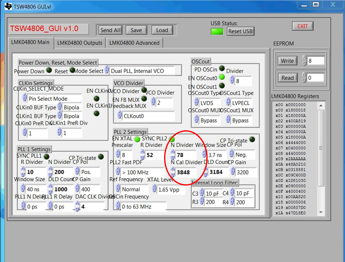
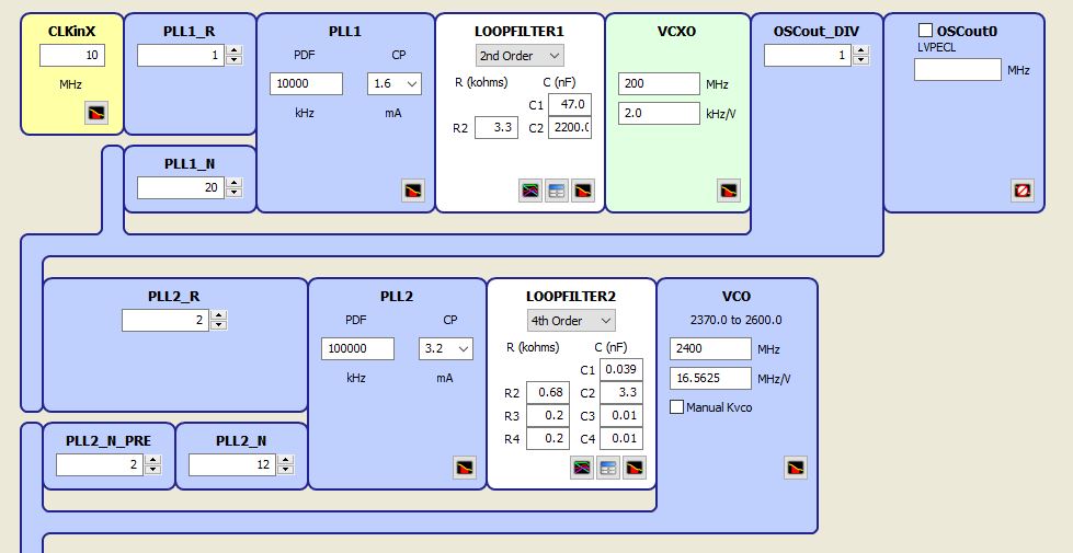
Y2 VCXO is installed for PLL2.  Captured configuration used shown as below.

I have included a document which shows the setting that he is using.

TSW4806EVM Frequency Issue.docx

It almost sounds like this is unstable. Can you look at the setting and see if the customer is doing anything wrong?

Thanks for your help with this!

Richard Elmquist

  • Hi Richard

    What are they using to provide the 10 MHz reference input to the board?

    What is the amplitude of the 10MHz signal and how much phase noise or jitter does it have?

    Best regards,

    Jim B

  • Jim,

    I will find out and respond back as quickly as I can.

    Thanks for your help with this!

    Richard Elmquist
  • Jim,

    Here is the response from the customer:

    What are they using to provide the 10 MHz reference input to the board?

    Since I am only using PLL2 with a 200MHz VCXO installed as an input source, my understanding is

    only VCXO specs becomes crucial.  Please confirm and see spec. attached.

    What is the amplitude of the 10MHz signal and how much phase noise or jitter does it have?

    Please refer to ABLJO spec. (200MHz, Voh = 0.9*VDD = 0.9*3.3, LVCMOS, 100fs rms jitter)

    I have attached the data sheet for the oscillator.

    TSW4806EVM Frequency Issue_ABLJO.pdf

    Thanks for your help with this!

    Richard Elmquist

  • Jim,

    Have you been able to look at the response from the customer?

    Please let me know if you have any further questions for the customer.

    Thanks for your help with this!

    Richard Elmquist
  • Richard,

    I have a feeling the 200MHz VCXO the customer installed is drifting. They need to use the 10MHz input reference to get this VCXO locked at exactly 200MHz using PLL1 of the device.

    Regards,

    Jim

  • Jim,

    Thanks for your reply!

    I will check with the customer and see if this fixes the issue. I will reply back as soon as I hear from them.

    Thanks for your help with this!

    Richard Elmquist
  • Jim,

    The customer has made the following comments and questions:

    Before revisiting the 10MHz-as-reference input suggestion, here are the comment/question I would like to make from previous attempts:

    Dual-loop PLL does require a 200MHz as an external source and that needs to specified.  

    How to bypass this requirement for using LMK048xx  is unknown to me.  See below capture.


    Can you or someone in your group provide a reference configuration setup besides the one used below ( which is suggested by TI), for me to try?

    I did not know how to answer him on this. Do we have another configuration that he can use?

    Thanks for your help with this!

    Richard Elmquist

  • Richard,

    This is GUI is from the clock group, not ours. I suggest you check with them.

    Regards,

    Jim
  • Jim,

    I have requested them to look at this.

    Thanks for your help!

    Richard Elmquist
  • Hi Richard,
    Customer wants to use the device in PLL2 mode only and wants to generate the PLL settings with Clock design Tool, is my understanding correct?
    If that is the case then they can specify the same frequency in the "Reference" & "VCXO1" field. The tool will then generate the settings for PLL1 & PLL2. They can then just use the configuration for PLL2 and ignore the settings for PLL1.
    Best regards
    Puneet
  • Puneet,

    The original issue was that the customer could not get the proper output frequency. If they wanted to generate 300 MHz they got 303 MHZ. When they programmed the device for 100 MHz they saw 101 MHz at the output.

    Jim Seton made a suggestion to the customer and the customer send in his questions that are shown above.

    Would this help the customer to see the proper output frequency? I just want to make sure before sending this to the customer.

    Thanks for your help with this!

    Richard Elmquist
  • Hi Richard
    If customer is trying to use the dual loop mode with VCXO, please ask them to share with me the registers setting they are programming. I think the PLL1 is not enabled correctly and is not locked. They can also use TICSpro tool to generate the register settings.
    If they want to use PLL2 only mode, then they can do what i said in my previous email.
    Best regards
    Puneet
  • Puneet,

    The customer is still having issues:

    I took your provided earlier suggestion by using an external 10MHz as an input.  I managed to have the PLL locked with the settings used as shown in figure1 below. These settings were derived from an example setting that came with the GUI installation and THIS SHOWED PLL LOCK (green LED "LOCK").  I also attached the setting_1111.txt for its register values used to configure the device (the settings below).

    LMK04800 Registers:
    
    0x00 0x1800018
    0x01 0x180000a
    0x02 0x400a819
    0x03 0x000000a
    0x04 0x000000a
    0x05 0x180000a
    0x06 0x4444000
    0x07 0x0400000
    0x08 0x4400000
    0x09 0x2aaaaaa
    0x0a 0x48a0210
    0x0b 0x0318881
    0x0c 0x09c600d
    0x0d 0x1d81030
    0x0e 0x0900000
    0x0f 0x4000400
    0x10 0x00aa820
    0x18 0x0000006
    0x19 0x0080800
    0x1a 0x47d18e0
    0x1b 0x08000c0
    0x1c 0x03e8180
    0x1d 0x0000f00
    0x1e 0x0000f00
    0x1f 0x0000000


    The only issue with this configuration setting is that the frequencies generated are not exactly what I want (245.xxMHz and 102.xxMHz: vs. 240MHz and 100MHz on clkout0 and clkout11 respectively).

    My questions:

    1.  What change can I make to this setting to get exactly 240MHz and 100MHz.
    2.  Why does the figure 2 configuration not show PLL "LOCK"? I am getting 266xxMHz and 111xxMHz, instead.

    I have attached a document which references the figure mentioned in the customer's response.

    TSW4806EVM Issue 11_7_17.docx

    Thanks for your help with this!

    Richard Elmquist

  • Puneet,

    Have you had time to look at the settings etc. that I attached in the previous email?

    Please let me know if you have any further questions for the customer.

    Thanks for your help with this!

    Richard Elmquist

  • Hi Richard

    Yes, i looked at the settings and i saw following issues:

    Setting 1: PLL1 N Divider should be 1920 ten PLL1 should lock. PLL2 settings are wrong. This will not give you 2400MH from 200MHz input.

    Settings 2: N Divider & N Cal Divider should be same (78 in this case).

    These are also not good settings for PLLs for performance.

    Please use the settings like in the snapshot below:

    Let me know if you still see any issue.

    Best regards

    Puneet

  • Puneet,

    Thanks so much for your thorough response!

    I will let you know if the customer has any further questions.

    Thanks so much.

    Richard Elmquist

  • Puneet,

    The customer is still having issues.

    Please look at the attached document as it shows the issue that they are still seeing.

    TSW4806_TI_OLYMPUS_LMK_EXCHANGE_rev1_11_13_17.docx

    Please let me know if you have any further questions from the customer as it seems that the settings are not working properly. Could they have a problem with the board?

    Thanks for your help with this!

    Richard Elmquist

  • Hi Richard,

    "Clock Design Tool" is a simulation tool for PLL loop parameters.

    After used it, we should use "TICS Pro", input setting according to previous simulation result.

    TICS PRo could generates registers map. It also could find similar settings in "TSW4806EVM GUI".

    Then you could get a correct setting.

    I found some problems in your application.

    1, OSCin frequency range setting should match 200 MHz.

    2, 3.3V LVCMOS is over spec. for LMK04806 VOSCin range 0.2~2.4Vpp.

    3, PLL dividers are wrong, PLL2 is unlock.

    4, 300 MHz LVCMOS is not supported by LMK04806.

    OSCin_200M_OUT0_1_100M_OUT2_3_300 MHz.zip

    Try attached setting, the .txt file could be loaded by TSW4806 GUI.

    If necessary, external loop filter RC also need to be changed on board.

    Regards,

    Shawn

  • Shawn,
    Thanks for your response!
    I will have the customer try this. I will let you know if this solves the issue.
    Have a great day!
    Richard Elmquist