This thread has been locked.

If you have a related question, please click the "Ask a related question" button in the top right corner. The newly created question will be automatically linked to this question.

ADS1243: ADS1243 interface with MSP432P401R controller

Part Number: ADS1243


Hello,

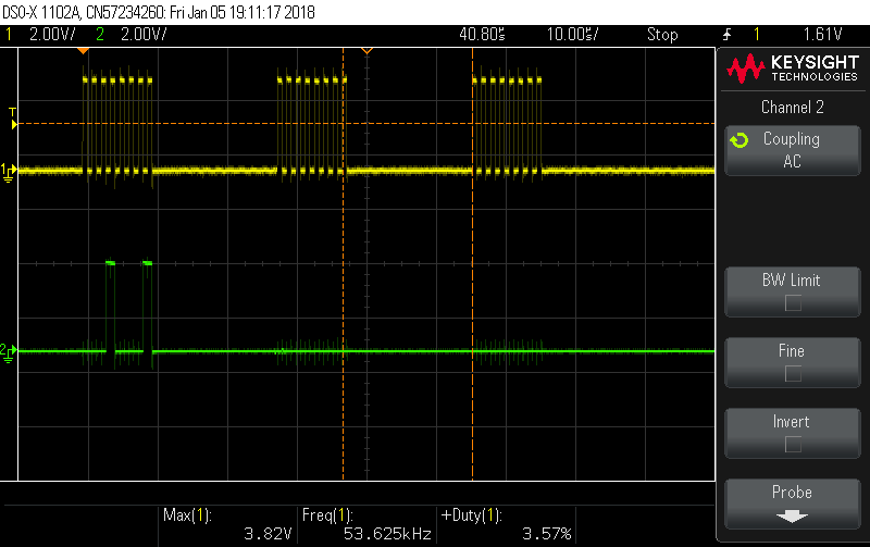
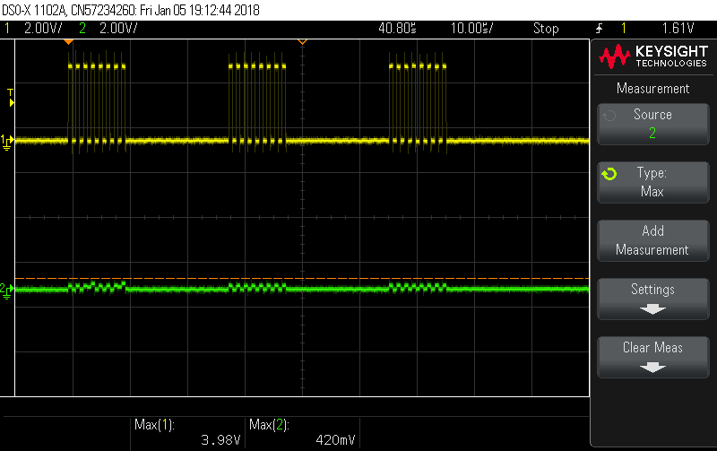
    I want to interface ADS1243 with MSP432P401R processor.ADS1243 is run @4.9152MHz external crystal.ADC work on 3.3V supply. Vref+ is +2.5V and Vref- is 0V(GND). If input voltage given to ADC is 1V then what should be the output data code??( output data code=Vin/(Vref/2^n-1)=666666H is right or wrong??)

 I am using default condition in register setup except speed bit and range bit is set to 1.SPI is working on 750kHz frequency.

Please check my code attached below and code sequence.

// MSP432P401M controller
/*
 * main.c
 * Created on: April 04, 2017
 */


#include "msp432p401m.h"
#include "ads1243.h"

void main(void)
{
    WDT_A->CTL = WDT_A_CTL_PW + WDT_A_CTL_HOLD;            // Stop WDT
    pin_init();
    dev_init_48M();
    dev_init_32k();
    InitDevice();
    InitSPI();
    InitDevice();
    InitSPI();
    ADS1243WaitForDataReady();
    ADS1243AssertCS();
    ADS1243SendByte();
    ADS1243ReceiveByte();
    ADS1243ReadData();
    ADS1243ReadRegister();
    ADS1243WriteRegister();
    ADS1243WriteSequence();
    ADS1243Speed();
    ADS1243Range();
    ADS1243SendSync();
 }


void InitSPI(void)
{
#if defined (__MSP432P401M__)

        EUSCI_B3->CTLW0 |= EUSCI_B_CTLW0_SWRST; // Put state machine in reset

        EUSCI_B3->CTLW0 = EUSCI_B_CTLW0_SWRST |
                EUSCI_B_CTLW0_SYNC |            // Synchronous mode
                EUSCI_B_CTLW0_CKPL |            // Clock polarity high
                EUSCI_B_CTLW0_MSB |             // MSB first
                EUSCI_B_CTLW0_MODE_1 |          // 4-pin SPI mode
                EUSCI_B_CTLW0_MST|              // master mode select
                EUSCI_B_CTLW0_STEM |            // STE mode select
                EUSCI_B_CTLW0_SSEL__SMCLK;      // SMCLK
        EUSCI_B3->BRW = 0x01;                   // /2,fBitClock = fBRCLK/(UCBRx+1).
        EUSCI_B3->CTLW0 &= ~EUSCI_B_CTLW0_SWRST;// **Initialize USCI state machine**
        while(!(UCB3IFG&UCTXIFG));          // Make sure nothing is already in the TX buffer
           UCB3TXBUF =0x55;    // 4-pin, 8-bit SPI slave
 #endif
}

void InitDevice(void)
{
#if defined (__MSP432P401M__)

    P10->SEL0 |= ADS1243_DIN + ADS1243_DOUT + ADS1243_SCLK;
    P2->SEL0 &= ~(ADS1243_DRDY);

    // define initial state
    P10OUT |= ADS1243_CS;

    // define inputs
    P2DIR &= ~(ADS1243_DRDY);                   // DRDY is an input to the micro

    // define outputs
    P10DIR |= ADS1243_CS;

#endif
}

/*
 * DRDY Polling Function
 * Timeout = 0 is wait until DRDY goes low no matter how long it takes, otherwise wait the specified number of cycles
 */
int ADS1243WaitForDataReady(int Timeout)
{
    /* This function shows a method for polling DRDY instead of using as interrupt function
     * -- Note: this method is not used in the demo, but if we the method was switched to polling from the interrupt method,
     * the desired port is PORT2 on the MSP430 as this demo is configured.
     */
    #if defined (__MSP432P401M__)
    if (Timeout > 0)
    {
        // wait for /DRDY = 1 to make sure it is high before we look for the transition low
        while (!(P2IN & ADS1243_DRDY) && (Timeout-- >= 0));
        // wait for /DRDY = 0
        while ( (P2IN & ADS1243_DRDY) && (Timeout-- >= 0));
        if (Timeout < 0)
            return ADS1243_ERROR;                   //ADS1243_TIMEOUT_WARNING;
    }
    else
    {
        // wait for /DRDY = 1
        while (!(P2IN & ADS1243_DRDY));
        // wait for /DRDY = 0
        while ( (P2IN & ADS1243_DRDY));
    }

#endif

    return ADS1243_NO_ERROR;
}

/*
 * Primary Low Level Functions
 */
void ADS1243AssertCS( int fAssert)
{
#if defined (__MSP432P401M__)
    // This example is using PORT10 for GPIO CS control, ADS1243_CS is defined in ADS1243.h
    if (fAssert){               // fAssert=0 is CS low, fAssert=1 is CS high
        _delay_cycles(50);      // Must delay minimum of 7 tosc periods from last falling SCLK to rising CS
        P10OUT |=  (ADS1243_CS);
    } else
        P10OUT &=  ~(ADS1243_CS);
#endif
}

void ADS1243SendByte(unsigned char Byte)
{
    char dummy;
#if defined (__MSP432P401M__)
    dummy = UCB3RXBUF;
    while(!(UCB3IFG&UCTXIFG));          // Make sure nothing is already in the TX buffer
    UCB3TXBUF =0x55;                    // Send the passed Byte out the SPI bus
    while(!(UCB3IFG&UCRXIFG));          // Before returning wait until transmission is complete and clear the RX buffer
    dummy = UCB3RXBUF;

#endif
}

unsigned char ADS1243ReceiveByte(void)
{
    unsigned char Result = 0;
#if defined (__MSP432P401M__)

  //  while(!(UCB3IFG&UCTXIFG));          // Make sure nothing is currently transmitting
  //  UCB3TXBUF = ADS1243_CMD_NOP;        // Send out NOP to initiate SCLK
    while(!(UCB3IFG&UCRXIFG));          // Wait until all data is transmitted (received)
    Result = UCB3RXBUF;                 // Capture the receive buffer and return the Result

#endif
    return Result;
}

long ADS1243ReadData(void)
{
    long Data;
    // assert CS to start transfer
    ADS1243AssertCS(0);
    // send the command byte
    ADS1243SendByte(ADS1243_CMD_RDATA);
    // get the conversion result
#ifdef ADS1243
    Data = ADS1243ReceiveByte();
    Data = (Data << 8) | ADS1243ReceiveByte();
    // sign extend data if the MSB is high (16 to 32 bit sign extension)
    if (Data & 0x8000)
        Data |= 0xffff0000;
#else
    Data = ADS1243ReceiveByte();
    Data = (Data << 8) | ADS1243ReceiveByte();
    Data = (Data << 8) | ADS1243ReceiveByte();
    // sign extend data if the MSB is high (24 to 32 bit sign extension)
    if (Data & 0x800000)
        Data |= 0xff000000;
#endif
    // de-assert CS
    ADS1243AssertCS(1);
    return Data;
}

void ADS1243ReadRegister(int StartAddress, int NumRegs, unsigned * pData)
{
    int i;
    // assert CS to start transfer
    ADS1243AssertCS(0);
    // send the command byte
    ADS1243SendByte(ADS1243_CMD_RREG | (StartAddress & 0x0f));
    ADS1243SendByte((NumRegs-1) & 0x0f);
    // get the register content
    for (i=0; i< NumRegs; i++)
    {
        *pData++ = ADS1243ReceiveByte();
    }
    // de-assert CS
    ADS1243AssertCS(1);
    return;
}

void ADS1243WriteRegister(int StartAddress, int NumRegs, unsigned * pData)
{
    int i;
    // set the CS low
    ADS1243AssertCS(0);
    // send the command byte
    ADS1243SendByte(ADS1243_CMD_WREG | (StartAddress & 0x0f));
    ADS1243SendByte((NumRegs-1) & 0x0f);
    // send the data bytes
    for (i=0; i < NumRegs; i++)
    {
        ADS1243SendByte(*pData++);
    }
    // set the CS back high
    ADS1243AssertCS(1);
}

void ADS1243WriteSequence(int StartAddress, int NumRegs, unsigned * pData)
{
    int i;
    char dummy;
    // set the CS low
    ADS1243AssertCS(0);
#if defined (__MSP430F5529__)
    // send the command byte
    dummy = UCB3RXBUF;
    while(!(UCB3IFG&UCTXIFG));          // Make sure nothing is already in the TX buffer
    UCB3TXBUF = ADS1243_CMD_WREG | (StartAddress & 0x0f);
    while(!(UCB3IFG&UCRXIFG));
    dummy = UCB3RXBUF;
    UCB3TXBUF = (NumRegs-1) & 0x0f;
    while(!(UCB3IFG&UCRXIFG));
    dummy = UCB3RXBUF;
    // send the data bytes
    for (i=0; i < NumRegs; i++)
    {
        UCB3TXBUF = *pData++;
        while(!(UCB3IFG&UCRXIFG));
        dummy = UCB3RXBUF;
    }

#endif
    // set the CS back high
    ADS1243AssertCS(1);
}

int ADS1243Speed(void)
{
    // write the register value containing the new value back to the ADS
    ADS1243WriteRegister(ADS1243_2_ACR , 0x01,ADS1243_SPEED_1);


}

int ADS1243Range(void)
{
    // write the register value containing the new value back to the ADS
    ADS1243WriteRegister(ADS1243_2_ACR , 0x01, ADS1243_SCALE_1);
}

void ADS1243SendSync(void)
{
    // assert CS to start transfer
    ADS1243AssertCS(0);
    // send the command byte
    ADS1243SendByte(ADS1243_CMD_DSYNC);
    // de-assert CS
    ADS1243AssertCS(1);
    return;
}


  • Sayali,


    With an input of 1V and a 2.5V reference and PGA Gain = 1, the output code is:

    666666h with RANGE bit = 1 or
    333333h with RANGE bit = 0

    The RANGE bit is BIT 2 in the ACR register.

    Are you having problems with reading out the device? If so, can you please describe that the problem you're having? Is the data completely wrong or do you have a gain or offset problem?


    Joseph Wu

  • Hi Joseph,
    I want to write and read the setup register value.but, I didn't get a sequence of reading and writing register of adc.I tried to write and read the setup register value using following sequence:-
    1) -cs is low
    write setup register
    - transmitt 0x50 value in TXBUF
    - TXBUF= 0x00(no of byte write to register)
    -TXBUF= 0x01(buffer disable and PGA is 2)
    -cs is high
    2) -CS low
    -transmitt dsync command i.e 0xFC in TXBUF
    -CS high
    3) wait for drdy getting low
    4) -CS low
    read setup register:-
    - TXBUF=0x10
    -TXBUF=0x00
    - check receive flag is clear or not and transmitt the receive data in variable"temp"
    when I debug the code the 0x01 value(value write in setup register ) is expect in receive buffer but the value is not getting.tell me exact code sequence?? Does any need to check drdy pin getting low??
  • Sayali,


    First, I would say that you should get an oscilloscope or logic analyzer to look at the SPI lines. It's important to know what the SPI lines are doing and it's far easier to debug problems with communications.

    I also want to say that I'm not the best at looking at code. Based on your explanation, I think that you're sequence is correct. However, at the beginning, I would insert a STOPC command first so that SPI communications aren't interrupted with a new data read.

    I did look through your code and there are two things that I noticed. First, I think you set CKPL to high. I think this should be 0. For the ADS1243, the SCLK idles low. Second, I don't see a setting for CKPH. Since the data is read on the falling edge of SCLK, I think you want to set CKPH to 1. You should be able to confirm this setup with an oscilloscope. Just review the timing diagram on page 6 of the datasheet.


    Joseph Wu
  • Hi joseph,

         As per your suggestions I make changes in my code. Still I cant read the register  data. Please check my code attached below:-

    // MSP432P401M controller
    /*
     * main.c
     * Created on: April 04, 2017
     */
    
    
    #include "msp432p401r.h"
    #include "ads1243.h"
    
    unsigned int Result=0;
    void main(void)
    {
        WDT_A->CTL = WDT_A_CTL_PW + WDT_A_CTL_HOLD;            // Stop WDT
        pin_init();
        dev_init_48M();
        dev_init_32k();
        InitSPI();
    
        P10OUT &=  ~(ADS1243_CS);          //CS LOW
    
        while(!(UCB3IFG&UCTXIFG));
        UCB3TXBUF =0x0F;                   //STOPC command transmit
        while(!(UCB3IFG&UCTXIFG));
        UCB3TXBUF =0x50;                   //write setup register
        while(!(UCB3IFG&UCTXIFG));
        UCB3TXBUF =0x00;                  //transmit no of register byte write
        while(!(UCB3IFG&UCTXIFG));
        UCB3TXBUF =0x08;                  // setup register data (BurnOut enable and PGA is 1)
        P10OUT |=  (ADS1243_CS);          //CS high
    
    
        P10OUT &=  ~(ADS1243_CS);           //CS LOW
        while(!(UCB3IFG&UCTXIFG));          // Make sure nothing is already in the TX buffer
        UCB3TXBUF =0x10;                    // read setup register
        while(!(UCB3IFG&UCTXIFG));          // Make sure nothing is already in the TX buffer
        UCB3TXBUF =0x00;                    // no of register byte read
    
        while(!(UCB3IFG&UCRXIFG));          // Wait until all data is transmitted (received)
        Result = UCB3RXBUF;                 // Capture the receive buffer and return the Result
        P10OUT |=  (ADS1243_CS);            //CS high
     }
    
    
    void InitSPI(void)
    {
    #if defined (__MSP432P401R__)
        P10->SEL0 |= BIT0 | BIT1 | BIT2| BIT3;  // set 4-SPI pin as second function
        P10->SEL0 &= ~(ADS1243_DRDY);
               P10DIR |=  BIT0 ;        //set CS as output
               P10OUT |=  BIT0 ;        //CS set high
               P2DIR  &= ~BIT5 ;        //DRDY as a input
    
            EUSCI_B3->CTLW0 |= EUSCI_B_CTLW0_SWRST; // Put state machine in reset
    
            EUSCI_B3->CTLW0 = EUSCI_B_CTLW0_SWRST |
                    EUSCI_B_CTLW0_SYNC |            // Synchronous mode
                    EUSCI_B_CTLW0_CKPH |            // Clock polarity high
                    EUSCI_B_CTLW0_MSB |             // MSB first
                    EUSCI_B_CTLW0_MODE_1 |          // 4-pin SPI mode
                    EUSCI_B_CTLW0_MST|              // master mode select
                    EUSCI_B_CTLW0_STEM |            // STE mode select
                    EUSCI_B_CTLW0_SSEL__SMCLK;      // SMCLK
            EUSCI_B3->BRW = 0x01;                   // /2,fBitClock = fBRCLK/(UCBRx+1).
            EUSCI_B3->CTLW0 &= ~EUSCI_B_CTLW0_SWRST;// **Initialize USCI state machine**
    
     #endif
    }


  • Sayali,


    To debug this, I would start by reading back all of the registers and not just the register that you've changed. This first tests if you're getting any reasonable value back (not just all 1s or 0s). It's also important to read something back that you expect. If you read FSR0, 1, and 2, you would know to expect 59 55 55. Regardless, read back all the registers and post what you have read from the device here. If you're not getting anything reasonable back from the device, you're SPI communication is broken. If that's the case, then writing to the device likely won't work either.

    Also, get an oscilloscope and make sure that the master is sending and receiving any SPI transmission. You could work on code this entire time and if the problem is in the hardware, you'll never find the issue. It's very important to look at the SPI lines coming in and out of the device.

    I don't see anything specifically wrong in your code, but as I mentioned earlier, I'm not an experienced programmer. However, if you want to, include the .h files in the next post.


    Joseph Wu
  • Hi,

    I just check SPI signals on DSO when data is transmitted:-

    -CS is high/low depending upon a code.

    -pulses are shown on SCLK pin

    - I tried to transmit 0x50 value in TXBUF and check signals on Din pin of ADS1243 on DSO .the value is transmitted successfully.it means, the value is written in ADC??

    -DRDY pin is shown active low on DSO.this pin is read only pin so it doesn't required to high or low through software(just wait for drdy getting low)?

    I am trying to read register value but, it its showing random value in RXBUF which i have been transmitted for reading the register. is there any need to transmit dsync and stop command for reading register.How to read register?? please tell me exact sequence..
  • Sayali,


    In your next post, can you please put up a scope shot of the spi communications so that I can read the transaction with the ADS1243? Show the /CS, DIN, DOUT, and SCLK lines and show enough detail so I can see the bit transactions.

    Before writing to the registers, start with reading them. To read the registers, it should be rather simple. First issue the STOPC command. Then read back the first three registers:

    The transaction should be:
    Bring /CS low
    Send 10 02 00 00 00
    During the last three bytes of 00 00 00, read the data.
    Bring /CS high.

    Use this transaction and record this with the oscilloscope and post it here.

    If you can do this, then writing to the device should be similar:
    Bring /CS low
    Send 50 00 xx (where xx is the data you want to write to the SETUP register)
    Bring /CS high.

    Unless you get everything working, please post the scope shots of the register read.


    Joseph Wu
  • Hi,
    I follow the sequence for reading the default register value.when I run the code, value receive d in RxBUF is 0x0F (stopc value).is there any need to provide some delay before read register??if yes then how much delay we have to provide??
    My spi is working on 750kHz frequency is right?? Because in datasheet they are not specify about spi frequency.

  • Sayali,


    Can you please post the scope shots of the communications? I'd like to see the SCLK, DIN, DOUT, and CS lines for each plot. I'd like to see the transactions for the STOPC command, and the RDATA that I'd requested. If you are writing to the device, post that as well. I need to be able to see the read back of data and verify what is coming on DOUT.

    An output of 0Fh doesn't translate to any register's default value in the device, and if you haven't written that to the device, then I'm not sure where it's coming from.

    Generally, there isn't a required delay between writing to and reading from the register. The register should be updated immediately. As for the SPI frequency, this is in the datasheet in the timing diagram specifications on page 6. The SCLK min period is 4 tosc. With a clock of 4.9152MHz, this translates to 0.813us for a period, and a max SCLK frequency of 1.23MHz. If there are problems writing to the device, t10 and t11 govern the min time from SCLK low to CS high, and the SCLK low to SCLK high after /CS has returned high. These two specifications are often overlooked. However look over the timing diagram and check to see if there are other possible problems. I don't think this is the root of the problems you're having, but it is important to review these values.

    Again, I would really like to see the scope shots of the communications.


    Joseph Wu
  • Hi;

    I removed external crystal & connect MSP.MCLK.P2.4 to ADS.Xin directly.The PDWN,CS,DRDY connected to GPIO pin .The ADC is being run at 3MHz (MCLK) and the serial communications are being clocked at SMCLK= 1.5MHz (MCLK/2).

    I am attaching  waveform of PDWN and DRDY signals which is checked on DSO:-

    1) Power down signal set high.

    2) On DRDy pin  pulses are  given after every 54mS:-


    3)SCLK gives a pulses when i tried to send continuous data.

    I am attaching a code and header file:-

    ads1243.h.docmain.doc

    Can you please ask any code expert and help me out to solve this issue?? 

  • Sayali,


    With an oscillator clock of 3MHz, the default data rate will be 18.31SPS. The equivalent data period is 54.6ms. In comparison to the /DRDY plot that you've posted, it looks like the ADC is operating and not in any kind of shutdown or reset mode.

    However, as I mentioned in the last post, the minimum SCLK period is 4*tosc. With a master clock frequency of 3MHz, the oscillator period is 333ns and the minimum SCLK period is 1.333us. This translates to a maximimum SCLK frequency of 750kHz. If you are using an SCLK frequency of 1.5MHz, it's still too fast. You will need to change this.

    As I also mentioned in the last post, it is still worth going through the timing characteristics table on page 6 of the datasheet. Even if someone else reviews the code, you'll need to know if your SPI communications violate any of the timing for the part.

    Also, I still think it is important to post the SPI communications from the device seen by the oscilloscope. This includes the SCLK, DIN, DOUT, and /CS communications when you write to and read from the device. You need to be able to see the signals and be able to read the data from the oscilloscope plots. At this point, the device seems to be converting. I think you should be able to read and write from the registers. With the scope plots, you should be able to see all register transactions, which would verify the data coming from the device. I think it is likely that the device is working, but there a problem with the MSP432 sending or receiving data. The scope plot could prove that out.

    However, if you need someone else to review your code, I would post into the MSP Low-Power Microcontroller Forum here:

    e2e.ti.com/.../166

    You can reference this post by copying the link.


    Joseph Wu
  • hi bob,

       in my code i change SPI frequency @750kHz as per your suggestion.i tried to read the default value of mux register is 0x01. but, the value is not received in receive buffer.I am attaching a screenshot of SCLK,DIN,DOUT waveform.

    1) SCLK(yellow colour) and Din(Green)

    2) SCLK  (yellow) and DOUT(green)

    please tell me why i cant read register value??

    this is code:-

    pin_init();
    dev_init_48M();
    dev_init_32k();
    P4DIR |= BIT3 ; // P4->3 set as output direction
    P4->SEL0 |= BIT3; // MCLK pin set @3MHz frequency
    InitSPI();


    P10OUT &= ~(ADS1243_CS); // CS LOW
    while(!(UCB3IFG&UCTXIFG)); // Make sure nothing is already in the TX buffer
    UCB3TXBUF =0x11; // read setup register
    __delay_cycles(50);
    while(!(UCB3IFG&UCTXIFG)); // Make sure nothing is already in the TX buffer
    UCB3TXBUF =0x00; // no of register byte read
    __delay_cycles(50);
    while(!(UCB3IFG&UCTXIFG)); // Make sure nothing is already in the TX buffer
    UCB3TXBUF =0x00; //00 to intialize clk
    __delay_cycles(50);
    while(!(UCB3IFG&UCRXIFG)); // Wait until all data is transmitted (received)
    Result = UCB3RXBUF; // Capture the receive buffer and return the Result
    P10OUT |= (ADS1243_CS); // CS high

  • Sayali,


    Thanks for posting the scope photos, I would like to have seen all four /CS, DIN, DOUT, and SCLK on the same plot, but this will work for now.

    I can already see that you have the wrong type of SPI communications set up from the MSP432. In your first plot the rising edges of the DIN are coincident with the falling edges of SCLK. This means that you have the MSP432 set up to communicate with the ADS1243 using SPI with CPOL=0 and CPHA=0.

    This needs to be changed so that the rising edges of DIN are coincident with the with the rising edges of SCLK. You should be using CPOL=0 and CPHA=1. This is shown in Timing Diagram 1 on page 6 of the datasheet.

    The way you have it set up, the MSP432 is changing the DIN just as the ADS1243 is trying to latch it in. It's unlikely that the ADS1243 is catching the correct bit.

    I would first change the MSP432 setup to correctly write to the device. I would also verify that /CS is low for the entire SPI transaction. If /CS returns high between the byte transactions, the SPI communication is reset and you still won't get the correct data out.


    Joseph Wu
  • Hello Joseph,

            I change the CKPL bit set to 0(The inactive state is low) and CKPH set to 0(Data is changed on the first UCLK edge and captured on the following edge). I am attaching a waveform of SCLK (yello) and DIN of ADC( green):-

    But still i cant get any data out from ads1243?? please help me??

  • Sayali,


    I still don't see what the problem is. The last scope photo shows the SCLK and DIN, which should have gotten a response from the ADS1243. However, you don't show the DOUT or the /CS on the plot. I really think it is important to show all the SPI communication to verify the timing. Do you have a four channel scope to show all the SPI lines at the same time?

    With SCLK and DIN shown together, it looks like the RREG command should be correct. The problem may not be specifically the code, but may be a physical problem like a broken connection or bad timing that isn't specifically noted in the program.

    However, we can review what works and what doesn't work at this point.

    First, it looks like the device is operational and converting. In your post of the /DRDY line, you can see that the device is putting out a pulse every 55ms. This shows that the device is enabled, not in sleep or reset.

    Second, you were able to read data based on your first post. This means that DOUT is connected to the master and that it does seem to respond to the SCLK. This means that both DOUT and SCLK seem to be connected and working. However, I haven't seen an oscilloscope plot of this yet. Are you still able to read the data? Plot this on the oscilloscope so I can see the timing. I want to make sure that SCLK and DOUT are still ok.

    Third, I'm not sure if DIN is operational. If you clocked out data before without RDATA, then issued STOPC, and then the data stopped, then it's likely that the DIN works. However, I haven't seen this on a scope shot, and I can't verify that DIN is working at all. You might also try reading a different register. If there were a timing issue and the SCLK is offset, you might miss reading the register. The 01h register has a default of 01h and if you missed an SCLK, you wouldn't see the last bit.

    Do you have a schematic you can share? One other thing that might help is to look at all the connections to see if there's anything that might interrupt the communications. I would verify that the communication connections of all SPI lines are valid. Again, this may not be a programming problem. I have looked through your code and at this point we really should verify everything about the SPI connections and timing of the communication.


    Joseph Wu
  • Hi joseph,

      i am attaching a screnshot of my circuit diagram:-

  • Sayali,

    Can you please provide a higher resolution copy of your schematic? I can't read any of the pin or node names in the circuit.

    As I mentioned in my last post, I still think it's important to show all communications from the SPI. I was hoping that you would be able to get a four channel scope to show /CS, DIN, DOUT, and SCLK at the same time. So far, you've only shown elements of two SPI lines, and it seems like nothing is coming out, but it's important to show all the lines.


    Joseph Wu

  • Sayali,


    I got another question from someone else about communication with the ADS1243. In the end, I was able to communicate with the device, but I did have two stumbling blocks. First, I missed a solder connection on DIN, which made it look like the device was receiving DIN, but it wasn't really getting it (a bad connection to SCLK would do the same thing). The second problem was that I had a timing violation. The timing for t6 (RREG SCLKs to the DOUT reading SCLKs) must be greater than 50tosc. This means that if the clock frequency is 2.45MHz, the time between the first byte and the second byte of the command must be greater that 20.4us.

    I couldn't control this with my master, but I increased the clock frequency to compensate. In your control, you should be able to set this time with the microcontroller.

    Regardless, I outlined the method I used to debug this in the following post:

    e2e.ti.com/.../2414272


    Joseph Wu