This thread has been locked.

If you have a related question, please click the "Ask a related question" button in the top right corner. The newly created question will be automatically linked to this question.

ADS1243: Reading and writing internal registers

Part Number: ADS1243
Other Parts Discussed in Thread: TMS320F28027,

Hello ,
I am using ADS1243 interfacing with TMS320F28027 launchpad.
Hardware Configration are

ADS1243 Side
Vdd-3.3 Vdc with respect to GND
Vref-1.23/1.24 Vdc[(REF IN+) = 1.24V abd (REF IN–) = GND]
Crystal oscillator between Xin and Xout of 4.9152 MHz (i have checked sine wave on oscilloscope when powerdown pin tie to vdd)
~CS connected to GND Directly
I have checked ~DRDY pulses which was of 33.60 mS (on+off -it low for more time than high) which is right according to datasheet.
And inputs are floating while reading register. I am not connecting any thing to adc in pins. I am using internal default condition to read register value.

Din-MOSI
Dout-MISO
Sclk to sclk
DRDY TO GPIO
POWERDOWN TO VDD
CS TO GROUND

Controller spi configration
Set to Master
Clock polarity- data out on rising edge and data in on falling edge(data in is doesn't matter as i am checking adc out signal on dso)
Spi clock at 500mhz
8 bit data transfer

Code sequence
Controller side Initialization (clock,pie and pie vector table )
SPI Initialization
Sent 0x11; //read internal registor
Delay of 16uS;
Sent 0x00; // single register read
Delay of 16uS;
Sent 0x00; // dummy byte send to genrate clock to receive data


In this conditions when i am sending data and checking on DSO it was correct with delay, 8 clock cycle and data on rising edge
But there is no data DOUT pin of ads1243
It was entirely high and my receive buffer of controller was filled with data of 0xFF as i am expecting 0x01 data in buffer

Is anyone have code sequence or working code.
I have try this sequence with different delay upto 100us but result was same.

  • Hello ,
    I am using ADS1243 interfacing with TMS320F28027 launchpad.
    Hardware Configration are

    ADS1243 Side
    Vdd-3.3 Vdc with respect to GND
    Vref-1.23/1.24 Vdc[(REF IN+) = 1.24V and (REF IN–) = GND]
    Crystal oscillator between Xin and Xout of 4.9152 MHz (i have checked sine wave on oscilloscope when powerdown pin connected to vdd)
    ~CS connected to GND Directly
    I have checked ~DRDY pulses which was of 33.60 mS (on+off -it low for more time than high) which is right according to datasheet.
    And inputs are floating while reading register. I am not connecting any thing to adc in pins. I am using internal default condition to read register value.

    Pin configuration of ADC To Controller 

    Din-MOSI
    Dout-MISO
    Sclk to sclk
    DRDY TO GPIO
    ~POWERDOWN TO VDD
    ~CS TO GROUND

    Controller spi configration
     Controller Set to Master
    Clock polarity- data out  from controller on rising edge and data in on falling edge(data in is doesn't matter as i am checking adc out signal on dso)
    Spi clock at 500MHz
    8 bit data transfer

    Code sequence
    Controller side Initialization (clock,pie and pie vector table )
    SPI Initialization
    Sent 0x11; //read internal registor
    Delay of 16uS;
    Sent 0x00; // single register read
    Delay of 16uS;
    Sent 0x00; // dummy byte send to genrate clock to receive data


    In this conditions when i am sending data from controller to adc and checking on DSO it was correct with proper delay, 8 clock cycle and data on rising edge
    But there is no data on DOUT pin of ads1243 when i am checking on DSO and rxbuffer
    DOUT pin was entirely high and my receive buffer of controller was filled with value of 0xFF(after masking into 8 bit)as i am expecting 0x01 data in buffer

    Is anyone have code sequence or working code.
    I have try this sequence with different delay upto 100us but result was same.
  • Ajay,


    If the /DRDY pulses are coming out, the device should be operational. This means that it's not in a sleep mode or in some sort of reset.

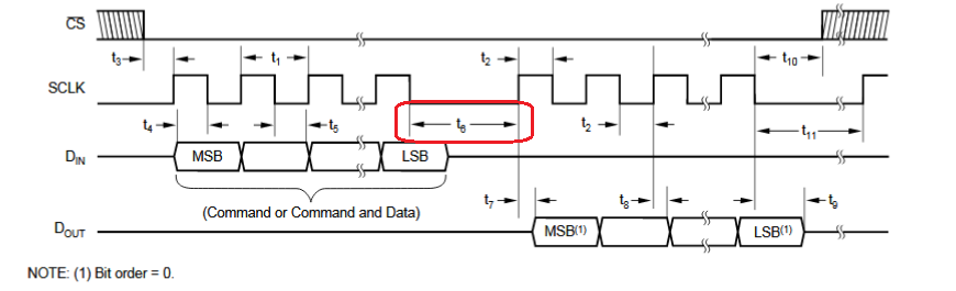
    The descriptions of your communications are correct. It looks like the SCLK period is ok based on the clock frequency. However, you need to verify all timing of the communications. The timing diagram is shown on page 6 of the datasheet. If you have used your DSO to look at this, post a scope shot of DIN, DOUT, and SCLK, presuming that you have tied /CS low.

    Note that tying /CS low may also lead to problems. If you have significant noise on SCLK, this will disrupt your SPI communications because the device may receive more SCLKs that you have sent. It may be difficult to recover from that error. You would need to run the SCLK reset waveform to reset the SPI communications. If you have a GPIO available, I would use the /CS.

    I would also verify your physical connections, checking to make sure you're measuring the correct pins and outputs. If you are able, can you please post a schematic to show your connections?


    Joseph Wu
  • Ajay,

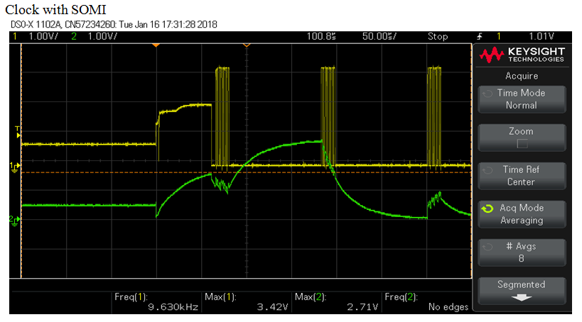
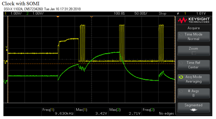
    I'm not sure what the problem is exactly, but I think your second plot shows quite a bit:

    DOUT appears to somehow float, which shouldn't be the case. For the ADS1243, the DOUT is actively driven (without the need for a pull-up or pull-down to read the device).

    I would check several things. First make sure that the master and slave have a common ground. GND needs to be the same for both devices. Check that the input to the scope is not set for AC coupling and is set for DC coupling. Last check that the connections from the slave to master are correct and that you are measuring the correct pin.

    If you continue to have problems, scope shots are very useful. It's best to try to get all four SPI lines in one shot (DIN, DOUT, SCLK, /CS). If you tie /CS low, then add /DRDY.

    Joseph Wu

  •  DearJoseph Wu,

    I have checked many time my hardware connections which are right (common ground,MOSI to Din ,MISO to Dout ,SCLK to SCLK and /CS with tied to ground and also i have tried /CS connected to /CS  with all condition master work properly).My DSO are set to DC coupling always when i am working with serial communication and i also verified it twice. I am taking care  and satisfying all the timing characteristics which are specified on page 6 of datasheet./power down pin is connected to VDD and /CS is connected to Ground and i have check Voltages on ADC which are right.

    I have tried resting device by RESET command and SCLK pattern with proper delay .Also i have tested Device with 5V VDD conditions and their Specified parameter according to datasheet. i am also change the chip and tested again.But every time i am getting same result.

    I dont have 4 channel DSO so i cant send you four signal at a time.earlier when i am trying following are the result on DOUT pin of ADC with clock with response of reading MUX resister.

    I have tested AD7730 chip with this launch pad with specified procedure in datasheet i am able to read and write proper data in that device. 

    Do you have any clear idea or any clear document about ADS1243 which contain all procedure to read/write internal register or any code sample which you tested with this device or any material which can help to read or write this data or read digital data from device, otherwise i have to proceed further with anything else.  

    do you have any tested code with this Device which i can try??

  • Ajay,

    Referring back to the following plot, I'd mentioned that this could be a floating ground.

    However, it could also be a large amount of capacitance on the DOUT pin to ground.

    I did spend some time today trying to read from the device, It did take some time, but I ended up getting the correct output from the device. I had two problems, one was a bad solder connection and the other was a timing error. Here's my process for getting the data out:

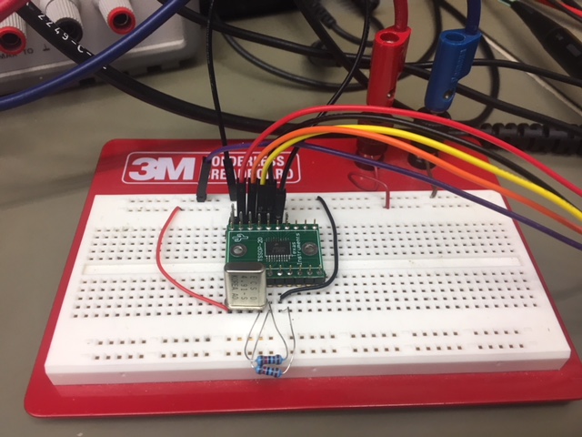
    I put together a small board with a Total Phase Aardvark as the master. Here is a picture of the board:

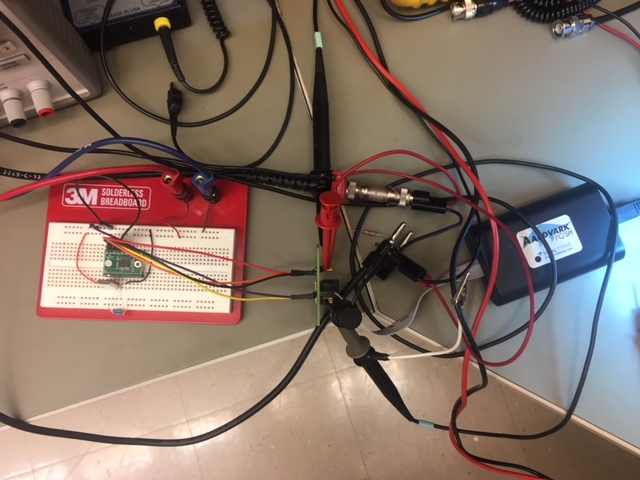
    And then a picture of the board with the Aardvark master:

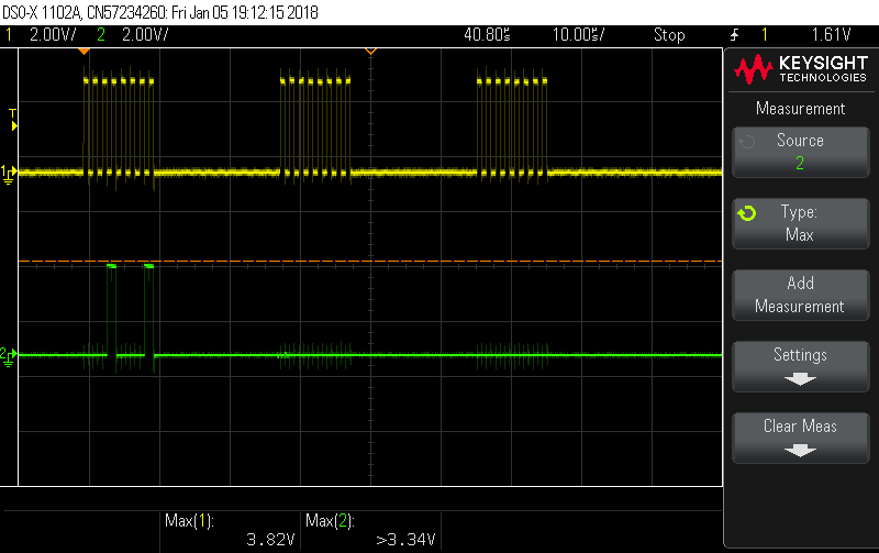
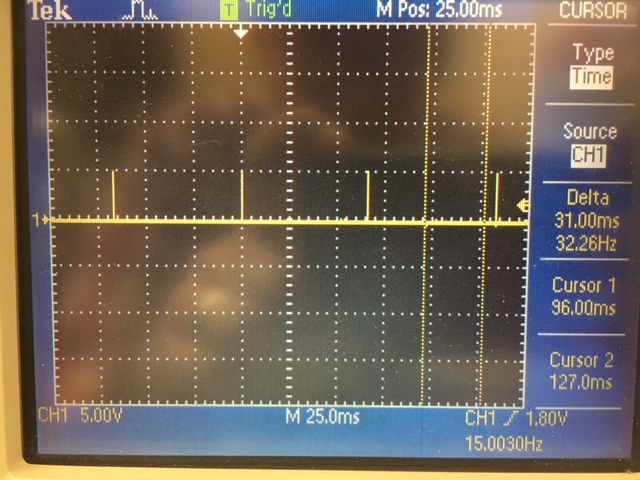
    First I start by looking at the /DRDY line when the device is powered up. I just want to make sure that the device is operational.

    Here, you can see that the /DRDY output is about 66uS, so that the data rate is 15SPS. In the end, I used a faster master clock (this one is 2.45MHz, and I eventually used 4.91MHz), but I'll get to that later. Again, this plot is to show that the device is operational.

    For a long time I was getting nothing on the DOUT. However as I mentioned, I had a problem with a bad solder connection on DIN. While I could see DIN from my probe connection, it wasn't getting to the device, so nothing was being clocked out.

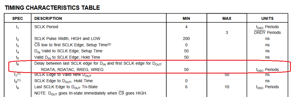
    I also found a problem in the SPI timing, if you look at the timing diagram on page 6, the time from a RREG command to the first SCLK edge for DOUT is 50tosc periods. This is about 20.5us. Unfortunately I can control SCLK frequency (which is set to the lowest setting of 125kHz), but I can't control the timing between the WREG byte to the DOUT read byte. The master sends out a bytes with a spacing of about 11us. To counter this, I had to speed up the master clock to 4.91MHz.

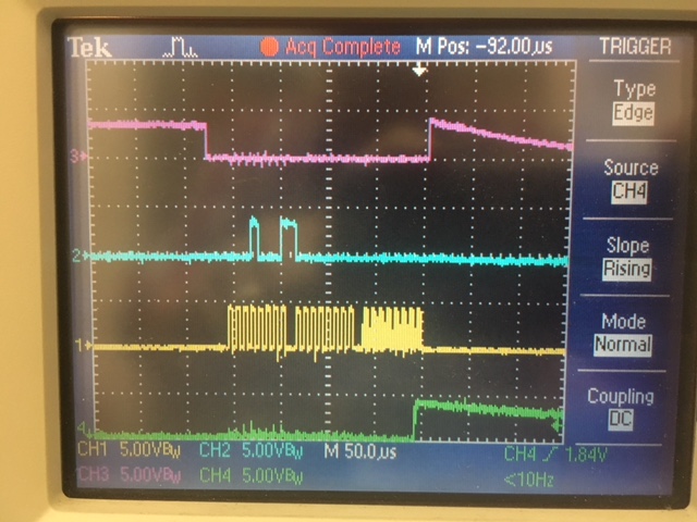
    In the end, Here is the output I got:

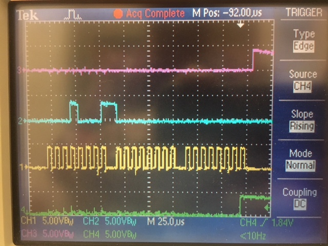
    Or if you look at it close up:

    Pink is /CS. Blue is DIN, Yellow is SCLK, and Green is DOUT. I this read, and I was able to read the full scale (gain) calibration register.

    To verify that the device was getting information, I used a couple of tricks. As I mentioned before, I verified that the device is operational by looking at the /DRDY line. If you monitor this line, you can also verify that the communication makes it to the device. If you send SLEEP (FDh) then the /DRDY pulses disappear. If you send SELFCAL (F0h) the /DRDY goes high for a little over 2 data periods as the device is calibrating. Regardless, this tests that you can write to the device.

    Again I used these tricks to determine the device receives the command. After that, I checked against the timing diagram to determine t6 was being violated.

    Regardless, you should be able to use similar methods to determine the communication problem.

    Joseph Wu

  • Dear Joseph,
    Thank you for you response. Can you send me your circuit diagram of ADC. As i can saw in images you have connected some component dear to crystal .i will try once with your setup .
  • Ajay,

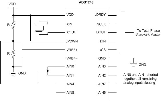
    I cobbled together test circuit with an ADS1243 mounted onto a TSSOP-20 board. This is a basic schematic:

    There's no precision reference, the inputs aren't designed to measure anything except offset, and there aren't any bypass capacitors. It's not what I'd use to build a precision measurement system, but I can use it to communicate with the device and take basic measurements if necessary.

    Note that my primary problem was this specification in the timing diagram:

    The t6 timing is longer than I would have expected. Apparently it takes longer for the device to parse the RDATA, RDATAC, RREG, and WREG commands before you communicate the part. I don't have the ability to control this with my master, that's why I increased my clock speed. If you're programming a microcontroller, you should be able to avoid this problem.

    Joseph Wu

  • Ajay,

    One other connection I forgot to mention in the diagram was the ground connection from the master to the slave board.

    The two must share a common ground, or the SPI communications may not work.

    Joseph Wu

  • Ajay,


    I just wanted to see if you were able to get a good read out of the ADS1243. If you weren't able to get a proper data or register read out of the device, post back with more details of your read error, and we can look at other things to debug. If you were able to read from the device, I'd like to close out this post.

    I'll leave the post open a little longer, but will close it soon. If you decide to post back and are locked out of this thread, feel free to start a new thread.


    Joseph Wu