This thread has been locked.

If you have a related question, please click the "Ask a related question" button in the top right corner. The newly created question will be automatically linked to this question.

ADS8691: Device configuration and register maps

Part Number: ADS8691
Other Parts Discussed in Thread: TINA-TI

Hi,

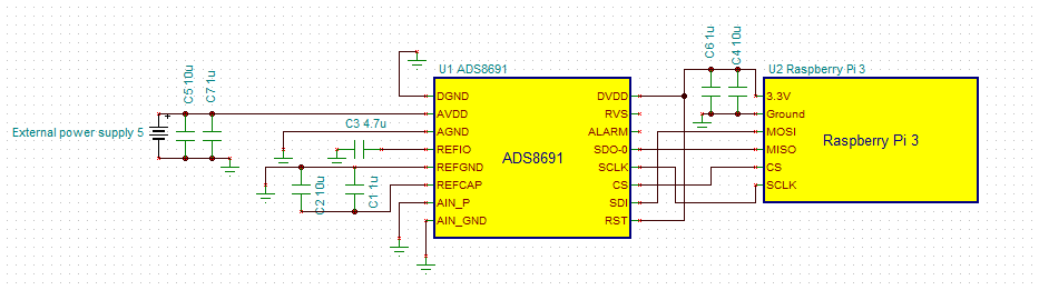
I've connected the ADS8691 as followed:

1 DGND -> 0V                                     16 DVDD->3,3V

2 AVDD ->   5V                                   15 RVS

3 AGND -> 0V                                    14ALARM/SDO-1/GPO

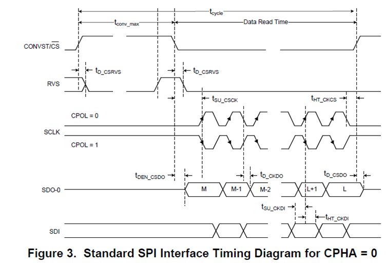
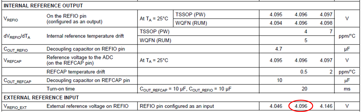
4 REFIO -> +4,7uF- -> ground           13 SDO-0 -> MISO

5 REFGND -> 1uF-, 10uF- and ground         12 SCLK -> SCLK

6 REFCAP -> 1uF+, 10uF+                            11 CONVST/CS -> GPIO pin

7 AIN_P ->                                          10 SDI -> MOSI

8 AIN_GND                                         9 RST -> GPIO pin 

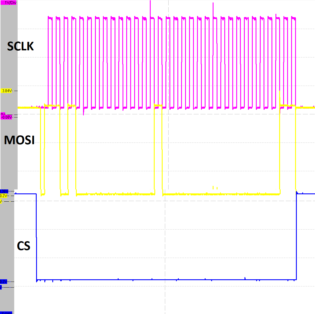
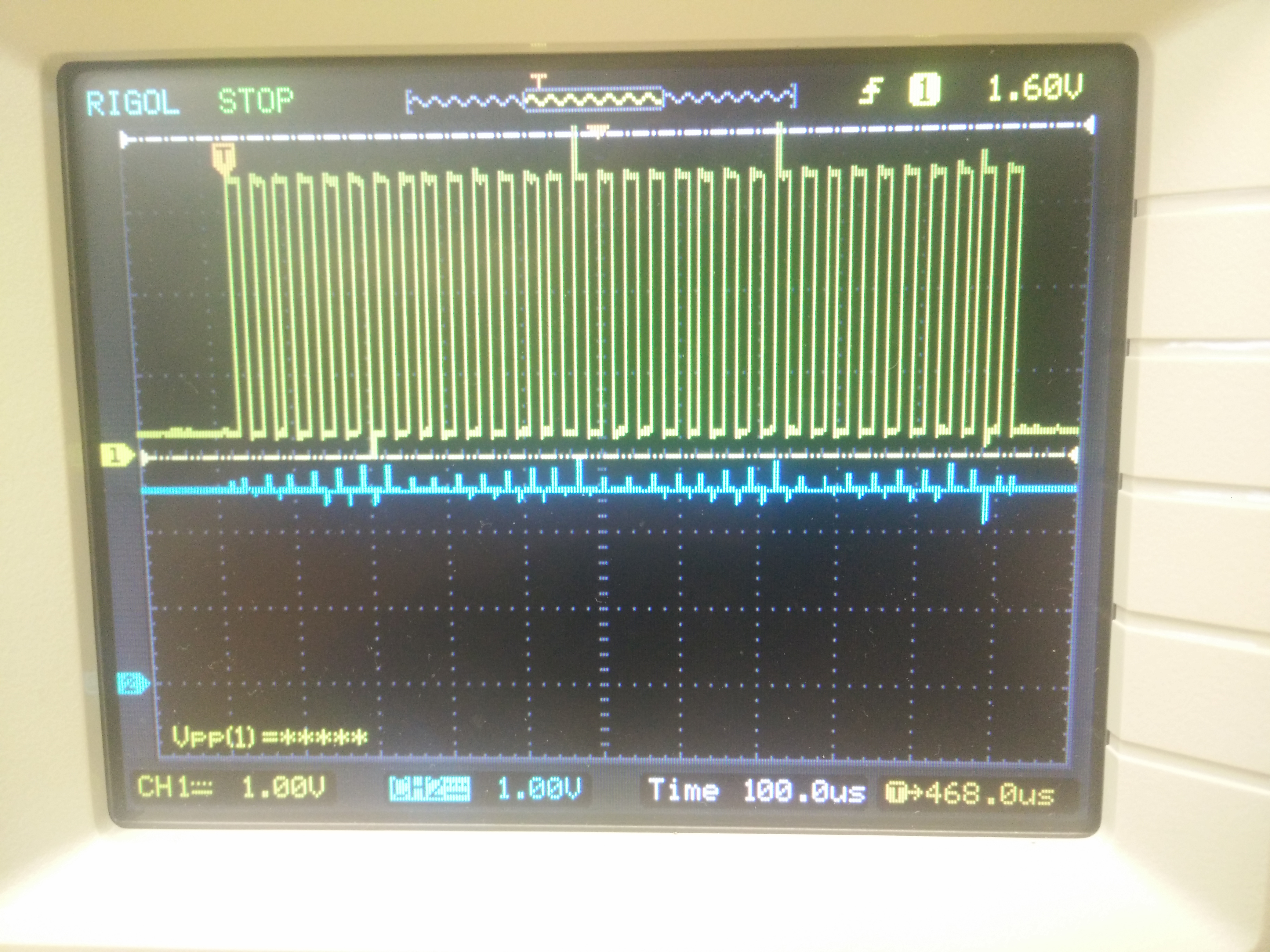
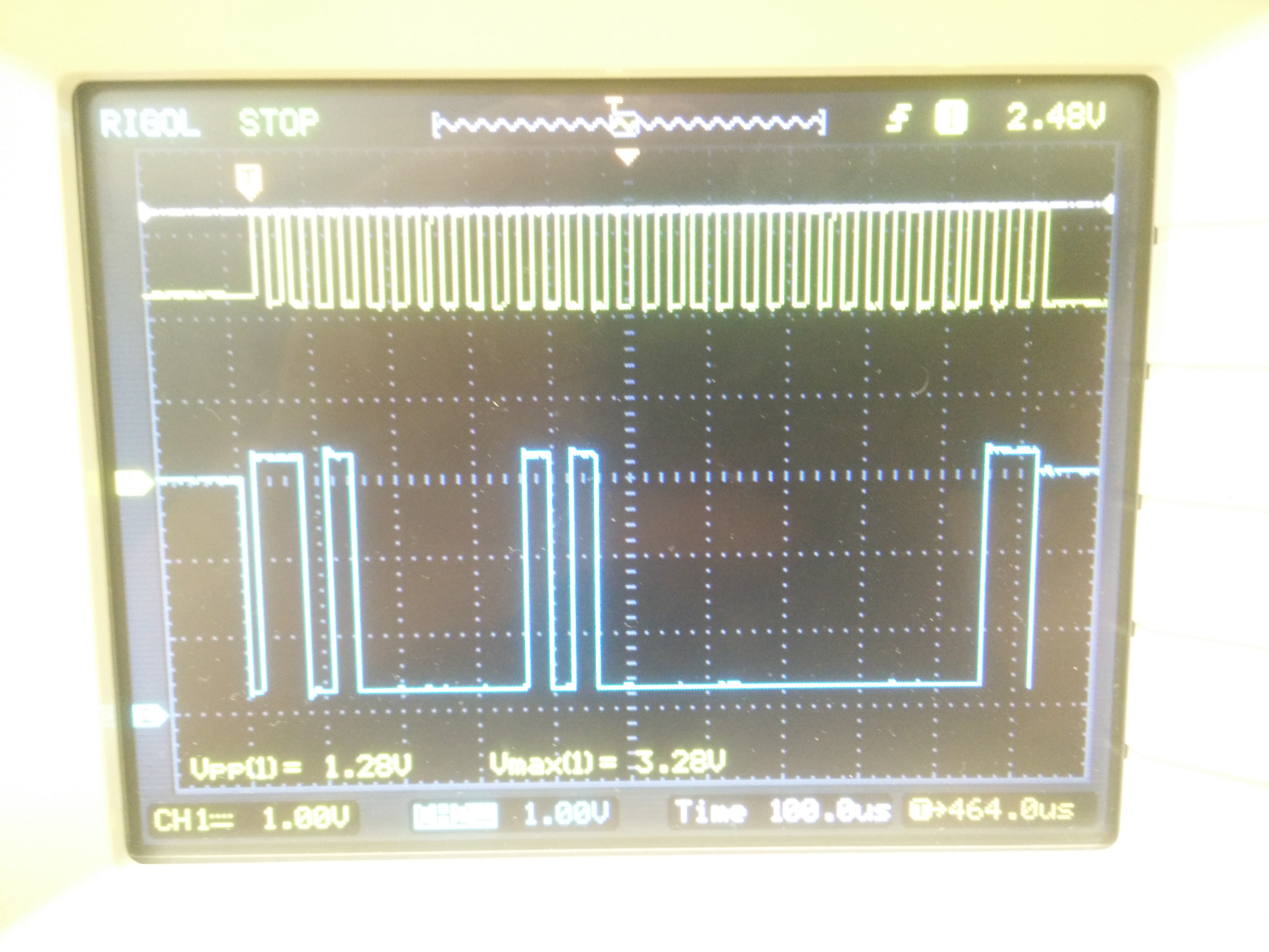
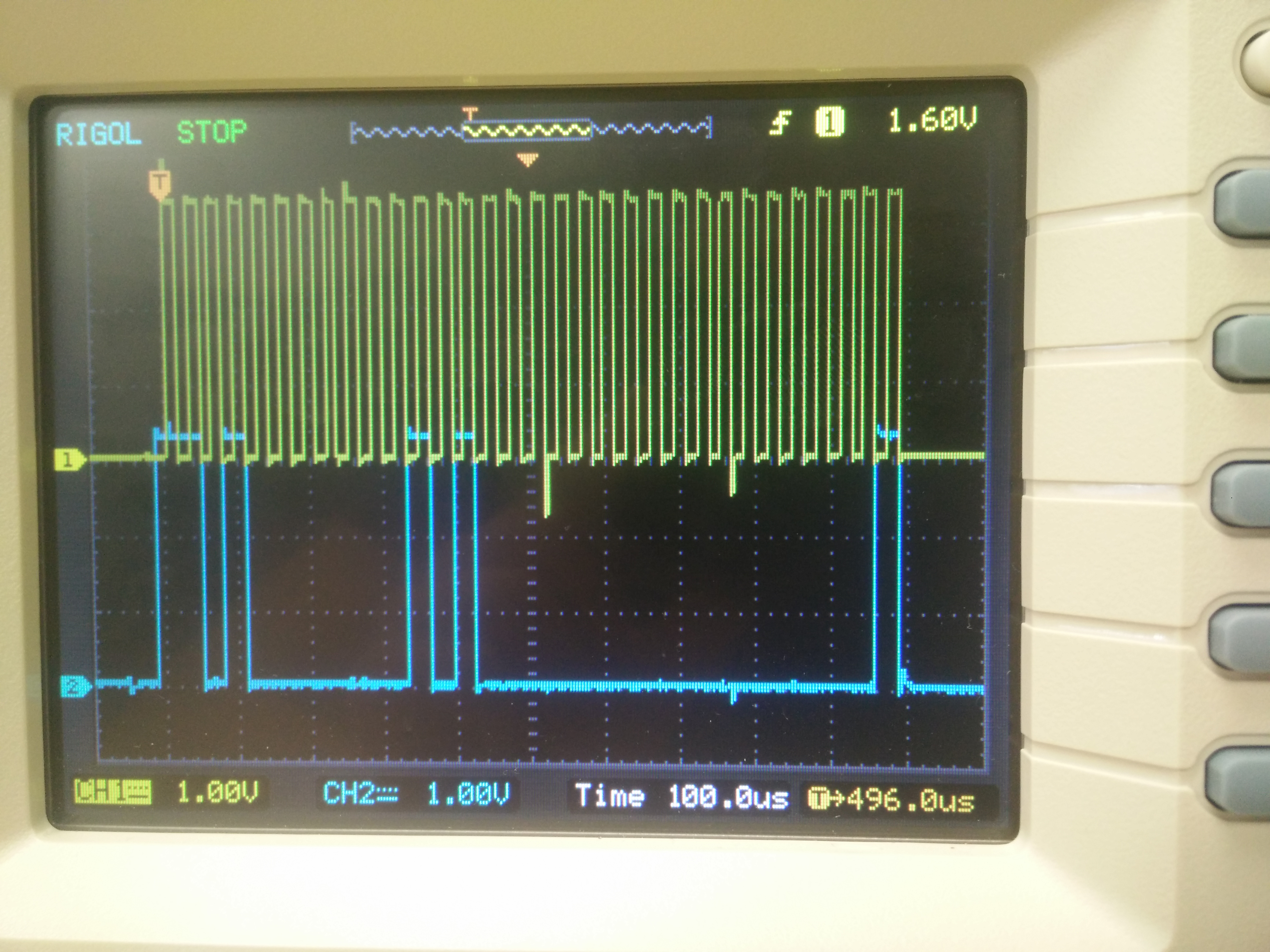
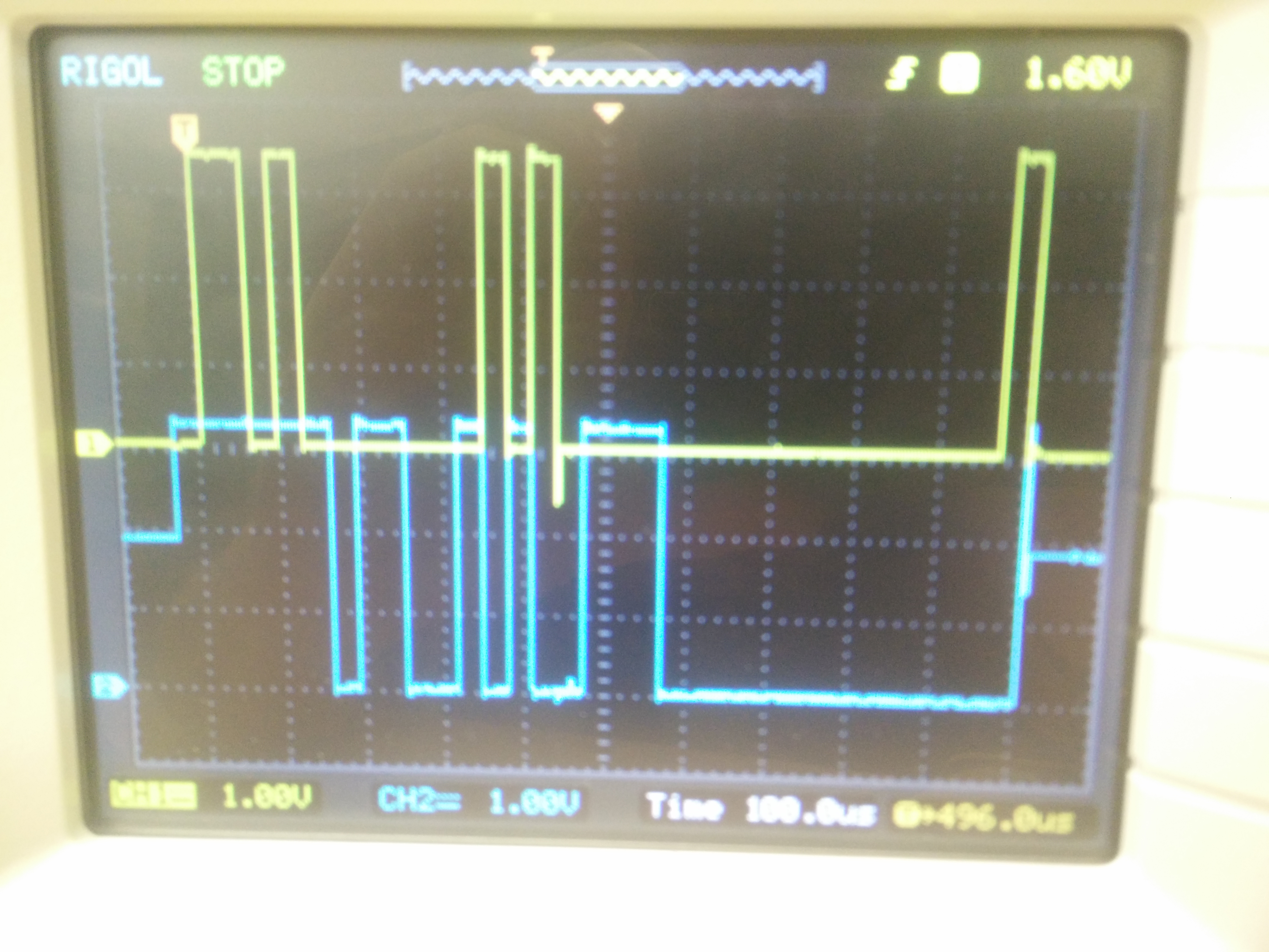
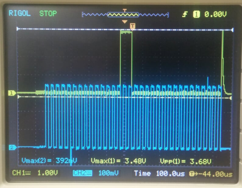
For some reason pin 10 (SDI) what suppose to be a digital input pin gives the value 3,3 Volt even when disconnected from MOSI. I only connected it as shown above.

Is this normal? I also experience a lot of noise on the SCLK.

Best regards

  • Hi Dukel,

    Thanks for your query on E2E forum.

    Your connection for SDI is fine because only specified OPCODEs can change the content of internal configuration registers, or you can have a pull-up resistor to DVDD as an option if you want.

    A clean SCLK is important to guarantee that your writing to and reading from ADC are successful because any data write operation to the device is always synchronous to the external clock provided on the SCLK pin and the data read from the device is synchronized to the SCLK clock as well (reading may use internal clock but still needs clock signals on RVS pin). There are timing requirements between SCLK, SDO and SDI, please refer to Figure 3-7 in datasheet.

    By the way, a minimum capacitance of 10μF must be placed between the REFCAP and REFGND pins. Place another capacitor of 1 μF as close to the REFCAP pin as possible for decoupling high-frequency signals, please refer to Figure 53 and 60 for details. You can upload your schematic to E2E for a review.

    Hopefully this is helpful to you.

    Best regards

    Dale

  • Hi Dale,

    I forgot to write the 10uF, but it was in place, I added it to my first post.

    The reason why I had so much noise on the SCLK was because I used both the 3.3V and 5V from the Raspberry to power the ADC. I'm now using a external 5V and there is no more noise on the SCLK.

    I'm sending a specified OPCODE to the ADC, but the configuration is not going well I think. could you check my code and the response.

    #include <stdio.h>
    #include <stdlib.h>

    #include <pigpio.h>

    //INPUT COMMAND WORD AND REGISTER WRITE OPERATION
    #define CLEAR_HWORD 0X6000
    #define READ_HWORD 0xC800
    #define READ 0x4800
    #define WRITE 0xD000
    #define WRITE_MS 0xD200
    #define WRITE_LS 0xD400
    #define SET_HWORD 0xD800

    //DEVICE CONFIGURATION AND REGISTER MAPS
    #define DEVICE_ID_REG 0x02 //Device ID register
    #define RST_PWRCTL_REG 0x04 //Reset and power control register
    #define SDI_CTL_REG 0x08 //SDI data input control register
    #define SDO_CTL_REG 0x0C //SDO-x data input control register
    #define DATAOUT_CTL_REG 0x10 //Ouput data control register
    #define RANGE_SEL_REG 0x14 //Input range selection control register
    #define ALARM_REG 0x20 //ALARM output register
    #define ALARM_H_TH_REG 0x24 //ALARM high threshold and hysteresis register
    #define ALARM_L_TH_REG 0x28 //ALARM low threshold register


    #define CONVST 22 //Pin 15 = BCM22 To activate reading on ADC
    #define RESET 18 //Pin 12 = BCM18 RESET

    #define uint32_t unsigned long long


    //VARIABLE
    unsigned char bytes[4];
    uint32_t data_to_receive;
    uint16_t ADC_Command = 0;
    uint32_t temp;

    //TEST VOID FUNCTION
    void Write_ADC(uint16_t ADC_Command, uint8_t byte2, uint8_t byte3)
    {

    bytes[0] = (uint8_t)(ADC_Command >> 8); //WRITE command
    bytes[1] = (uint8_t) ADC_Command; //Register Address
    bytes[2] = (uint8_t) byte2; //
    bytes[3] = (uint8_t) byte3; //2.5*Vref and internal reference enabled
    spiXfer(0, (char *)(&bytes), (char *)(&data_to_receive), 4);
    }

    int main(int argc, char *argv[])
    {


    gpioInitialise(); //Initialise pigpio.h

    spiOpen(0,32000,0);
    gpioSetMode(CONVST, PI_OUTPUT); //Chip select (ADC)
    gpioSetMode(RESET, PI_OUTPUT); //Reset ADC

    while(1){
    //Configure ADC
    gpioWrite(CONVST,1);
    gpioSleep(PI_TIME_RELATIVE, 0, 500000); //0.5second delay

    //~ //CONFIGURES THE PROTOCOL USED FOR WRITING DATA TO THE DEVICE
    //~ gpioWrite(CONVST,1); //Set high
    //~ gpioDelay(0.0095);
    //~ gpioWrite(CONVST,0); //pull low to initiate a data transfer frame
    //~ gpioDelay(0.0095);
    //~ //BEGIN CONVERSION
    //~ Write_ADC(WRITE+SDI_CTL_REG, 0x00, 0x01); //CPOL=0 AND CPHA=1
    //~ //END CONVERSION
    //~ gpioWrite(CONVST,1); //pulls high to end the data transfer frame
    //~ gpioDelay(0.665); //wait for tCONV_max to elapse before initiating a new data transfer frame (665ns)

    //~ /* SAME AS RESET MODE
    //~ //CONTROLS THE DATA PROTOCOL USED TO TRANSMIT DATA OUT FROM THE SDO-x
    //~ gpioWrite(CONVST,0); //pull low to initiate a data transfer frame
    //~ gpioDelay(0.0095);
    //~ //BEGIN CONVERSION
    //~ Write_ADC(WRITE+SDO_CTL_REG, 0x00, 0x00); //SDO_MODE same as SDI, SSYNC_CLK external, SDO1_CONFIG tri-stated, GPO_VAL 1-bit
    //~ //END CONVERSION
    //~ gpioWrite(CONVST,1); //pulls high to end the data transfer frame
    //~ gpioDelay(0.665); //wait for tCONV_max to elapse before initiating a new data transfer frame (665ns)
    //~ */

    //Set ADC input Range and Internal reference. Decimal value should be: 3490971649, Binary: 1101 0000 0001 0100 0000 0000 0000 0001
    gpioWrite(CONVST,0); //pull low to initiate a data transfer frame
    gpioDelay(0.0095); //0.0095
    //BEGIN CONVERSION
    Write_ADC(WRITE+DEVICE_ID_REG, 0x00, 0x03); //RANGE_SEL 2.5*Vref, INTREF_DIS enabled
    //WAIT FOR 32-BIT

    //END CONVERSION
    gpioDelay(0.665); //wait for tCONV_max to elapse before initiating a new data transfer frame (665ns)
    gpioWrite(CONVST,1); //pulls high to end the data transfer frame

  • It looks like it is sending information back to the MCU but because the  SDO is always high even when not connected to the MCU, it can't read anything.

    Yellow: SCLK
    Blue: SDO

    Do I need to put a pull-down resistor on it?

  •  Hi Dukel,

    You are trying to set ADC input Range and Internal reference (RANGE_SEL 2.5*Vref, INTREF_DIS enabled), but you are writing 16-31 bit of  DEVICE_ID_REG(0x02) as below, actually 16-19 bits in this register are only available in daisy-chain mode and 20-31 are reserved in this register.

    "Write_ADC(WRITE+DEVICE_ID_REG, 0x00, 0x03); //"

    This is why your configuration was not successful, also I didn't see you have any available Read command to read internal register, so you could not get anything back to MCU.

    Best regards

    Dale

  • Hi Dale,

    You are right, I copied the wrong part!

    This is my code, In the image below you can see the new response. Top line (yellow) is the SDI and it is behaving like a clock or something.

    gpioInitialise(); //Initialise pigpio.h

    spiOpen(0,32000,0);
    gpioSetMode(CONVST, PI_OUTPUT); //Chip select (ADC)
    gpioSetMode(RESET, PI_OUTPUT); //Reset ADC

    bytes[0] = 0;
    bytes[1] = 0;
    bytes[2] = 0;
    bytes[3] = 0;

    while(1){
    //Configure ADC
    gpioWrite(CONVST,1);
    gpioDelay(0.0095);
    //gpioSleep(PI_TIME_RELATIVE, 0, 500000); //0.5second delay


    //Set ADC input Range and Internal reference. Decimal value should be: 3490971649, Binary: 1101 0000 0001 0100 0000 0000 0000 0001
    gpioWrite(CONVST,0); //pull low to initiate a data transfer frame
    gpioDelay(0.0095); //0.0095
    //BEGIN CONVERSION
    Write_ADC(WRITE+RANGE_SEL_REG, 0x00, 0x03); //RANGE_SEL 2.5*Vref, INTREF_DIS enabled
    //WAIT FOR 32-BIT

    //END CONVERSION
    gpioDelay(0.665); //wait for tCONV_max to elapse before initiating a new data transfer frame (665ns)
    gpioWrite(CONVST,1); //pulls high to end the data transfer frame
    gpioDelay(0.665);

    printf("%llu first \n",data_to_receive);
    gpioSleep(PI_TIME_RELATIVE, 0, 100000);

    //PREFORM A 16-BIT READ OPERATION
    gpioWrite(CONVST,0); //pull low to initiate a data transfer frame
    gpioDelay(0.0095);
    //BEGIN CONVERSION
    Write_ADC(READ_HWORD+RANGE_SEL_REG, 0x00, 0x00); //
    //END CONVERSION
    gpioDelay(0.665);
    gpioWrite(CONVST,1); //pulls high to end the data transfer frame
    gpioDelay(0.665); //wait for tCONV_max to elapse before initiating a new data transfer frame (665ns)

    printf("%llu second \n",data_to_receive);
    gpioSleep(PI_TIME_RELATIVE, 0, 100000);

  • Could you please help me with this? For some reason the SDO is sending a clock signal instead of data and it is kept high, it only varies 1 Volt.

    Best regards,
    dukel
  • Hi Dale,

    The problem with the SDI is solved. it is no longer coping the clock an it gives a full range output. What he is sending back is not clear to me but in the following image you can see that is send the value: 3490971649 or in binary: 1101 0000 0001 0100 0000 0000 0000 0001 with the command:  Write_ADC(WRITE+RANGE_SEL_REG, 0x00, 0x01); 

    The image below shows that it is really sending the right information to the ADC.

    If I only send: Write_ADC(WRITE+RANGE_SEL_REG, 0x00, 0x01); Than receive this: (yellow is what i'm sending)

    I Tried the following code and i expected upon the last command to receive 16-bits that represents the RANGE_SEL_REG configuration. What am I doing wrong with the read.

    //Set ADC input Range and Internal reference. Decimal value should be: 3490971649, Binary: 1101 0000 0001 0100 0000 0000 0000 0001
    gpioWrite(CONVST,0); //pull low to initiate a data transfer frame
    gpioDelay(0.0095); //0.0095 = 9.5ns
    //BEGIN CONVERSION

    Write_ADC(WRITE+RANGE_SEL_REG, 0x00, 0x01); //RANGE_SEL +-2.5Vref INTREF_DIS enabled

    //WAIT FOR 32-BIT

    //END CONVERSION
    gpioDelay(0.665); //wait for tCONV_max to elapse before initiating a new data transfer frame (665ns)
    gpioWrite(CONVST,1); //pulls high to end the data transfer frame
    gpioDelay(0.665);

    printf("%llu first \n",data_to_receive);
    gpioSleep(PI_TIME_RELATIVE, 0, 100000);


    //PREFORM A 16-BIT READ OPERATION
    gpioWrite(CONVST,0); //pull low to initiate a data transfer frame
    gpioDelay(0.0095);

    //BEGIN CONVERSION
    Write_ADC(READ_HWORD+RANGE_SEL_REG, 0x00, 0x00); //

    //END CONVERSION
    gpioDelay(0.665);
    gpioWrite(CONVST,1); //pulls high to end the data transfer frame
    gpioDelay(0.665); //wait for tCONV_max to elapse before initiating a new data transfer frame (665ns)

    printf("%llu second \n",data_to_receive);
    gpioSleep(PI_TIME_RELATIVE, 0, 100000);

    //READ 16-BIT FRAME THAT IS BEING SEND AFTER READ_HWORD
    gpioWrite(CONVST,0); //pull low to initiate a data transfer frame
    gpioDelay(0.0095);

    //BEGIN CONVERSION
    Write_ADC(READ_HWORD, 0x00, 0x00); //

    //END CONVERSION
    gpioDelay(0.665);
    gpioWrite(CONVST,1); //pulls high to end the data transfer frame
    gpioDelay(0.665); //wait for tCONV_max to elapse before initiating a new data transfer frame (665ns)

    printf("%llu thirth \n",data_to_receive);
    gpioSleep(PI_TIME_RELATIVE, 0, 100000);

  • Hi Dukel,

    I will get back to you soon.

    Thanks&Regards

    Dale

  • Hi,

    What do I need to do to receive the digital data that should represent the analogue value of the sensor. Even without configuring the device, in default it should already convert the analogue value to a digital one right?

    Do I need to write 32 times 0 which stands for No operation and equals the "All other input command combinations" command. Or do I have to give a READ / READ_HWORD command followd by some kind of address to receive the digital data over ADC SDO-0?

    Right now I'm sending (1100 1000 0000 0010 0000 0000 0000 0000) which stands for READ_HWORD followed by RANGE_SEL_REG and 16 times 0
    After that command to read the configuration of the range and reference I send 32 times 0 over de SPI.
    I think this would result in first sending the read command over the SDI and at the next 32-bit  get the configuration back via the SDO. Is this interpretation right?

    I also tried sending a READ_HWORD only, so: 1100 1000 0000 0000 0000 0000 0000 0000 is send to the SDI and visible on my scope. This results in a constant value which is send back to my Raspberry Pi (also visible on my scope), but does not change when I change the sensor input value to for example 3V or 0V

    Performing only a spiRead, so not sending anything but only receiving results in what looks like random numbers

    Regards,
    Dukel

  • Hi Dukel,

    You can get conversion data without any register programing, the ADC and internal registers have default status as below after power up:

    Input range:    ±3 × VREF

    Reference:      Internal reference is enabled

    SDI_MODE:   00b = Standard SPI with CPOL = 0 and CPHASE = 0

    If you are using internal voltage reference, check the voltage on REFIO and REFCAP to make sure they are 4.096V. You need to send SCLK clocks to shift out the data to SDO line after you make /CS low, writing 0 on SDI is a good way to have SCLKs to ADC. Check if RVS has a output, please refer SCLK,RVS and /CS as below figure 3 or figure 4 in datasheet.

    In your tests:

    • When you sending “(1100 1000 0000 0010 0000 0000 0000 0000) which stands for READ_HWORD followed by RANGE_SEL_REG and 16 times 0”, you are trying to read DEVICE_ID_REG Register because the register address you are sending is 0x02h, which is not RANGE_SEL_REG’s address, you are reading 16-31 bit of DEVICE_ID_REG Register(Reserved bits and Device_ADDR bits), all 0s value read back from ADC are correct. You are sending wrong address for the register you want
    • When you sending “READ_HWORD only, so: 1100 1000 0000 0000 0000 0000 0000 0000”, you are reading 0-15 bit of DEVICE_ID_REG Register which are all reserved bits, all 0s value read back from ADC are correct as well.

    If a valid READ/ READ_HWORD command is issued in frame F, the output data word for frame (F+1) contains 8-bit/16-bit register data, followed by 0's. Please notice that you can only get the register data in next frame(F+1), not frame F.

    Best regards

    Dale

  • Hi Dale,

    Thank you for your reply. I recon that I'm doing it wrong. Would this be correct for READ_HWORD and RANGE_SEL_REG:

    (14h = 20 in decimal)

    1100 1000 0001 0100 0000 0000 0000 0000 = 3356753920   
    OR
    1100 1000 0010 1000 0000 0000 0000 0000 = 3358064640 (because the address is 9-bits and the LSB is ignored)

    for reading the Address for bits 7-0 = 14h

    RVS is going low while sending/reading data, so that is going well.

    Thing is. The internal reference does not equal 4.096. I'm supplying the AVDD with 5V and the DVDD with 3.3V. The voltage across REFCAP - REFGND fluctuates a bit and is 4.6V

    Best regards,
    Dukel


  • Hi Dukel,

    1100 1000 0001 0100 0000 0000 0000 0000 is correct command to read bit 0-15 of Range_SEL_REG register..

    What's the voltage on REFIO pin?

    Thanks.

    Regards

    Dale

  • Hi Dale,

    When the voltage between REFCAP- REFGND equals 4.65V, the voltage across REFIO and Ground is 4.55V. A 4.7uF capacitor is connected between REFIO and ground.

    While running the voltage over REFCAP - REFGND is pretty stable (4.61V) but the conversion to a digital signal is not that accurate. When I ground the input signal the decimal outcome fluctuates between 130849 and 124349 approximately. This is close to the halve of 2^18 which is 262144/2 = 131072 but I expected it to be closer and more stable 

    Regards,

    Dukel

  • Hi Dukel,

    The voltage on REFIO should be 4.096V when internal reference is used, something is wrong with your circuit, can you send me your schematic?

    Best regards

    Dale

  • Sure, this is it. I couldn't find a model for the ADS8691 for in TINA-TI.

    Regards,

    Dukel

  • Hi Dukel,

    If this is your real schematic, definitely the voltage measured on REFIO pin should be about 4.096V after power up (+5V from external supply and +3.3V from Raspberry Pi 3 Embedded System Development Board), it should not be 4.55V as you mentioned above. Can you please replace the ADC with a new ADS8691 device?

    Regards

    Dale

  • Hi Dale,

    I have another ADS8691, so I will swap the ADC and check if the REFIO measures 4.096 V.

    Would it be possible the connect an external reference of say 1 Volt to the ADS8691, or does is have to be 4.096 Volt?

    Regards,
    Dukel
  • Hi Dukel,

    To achieve the performance specified in datasheet, you have to use 4.096V external voltage reference or use internal 4.096V reference, refer to below requirement screenshot from datasheet:

    Please take a look at the datasheet for more details, thanks.

    Best regards

    Dale

  • Hi Dale,

    I did look at the datasheet but the part about the external reference was a bit confusing. the max rating says that REFIO could be between -0.3V - 7V.

    It's now clear that when using an external reference the input can only be 4.046 - 4.146V

    I swapped the ADC and this only gives 1 V or less on REFIO. I soldered it myself en did a continuity test to check if all pins where connected and no bridge between pins. 
    AVDD = 4.76V

    I measured the resistance between several pins on both the new and old ADS891.

    old new
    Connected  like above circuit (no power)
    sclk AGND 53,3kohm 25,3kohm
    REFCAP REFGND 6.14Mohm 120kohm
    REFIO REFGND 1.2Mohm 42kohm
    Not connected
    sclk AGND 17Mohm 9Mohm
    REFCAP REFGND >20Mohm 0.250Mohm
    REFIO REFGND >20Mohm 0.225Mohm

    I have no idea why this is different. I've been very careful with the ADC's. always waring a ESD protection and preformed a continuity test before connecting to power.
    Could you take a look what the readings you're getting?

    Something else is not going according to plan.

    While sending a READ_HWORD with RANGE_SEL_REG (11001000000101000000000000000011 sets the input range to 1.25*Vref ) I expected to receive the result (00000000000000110000000000000000) in the next frame, which also getting. see figure below (Blue is clock, yellow SDI).

    but when I'm reading the sensor results, I'm still getting the same value for 0 or 5 Volt as in default mode (3*Vref)

    Regards 

  • Hi,

    The Absolute Max Rating table is specified for the voltage/current which will not lead to any damage to the device. To make the ADC proper working and get the specified performance in datasheet, you will have to use recommended conditions in Electrical Characteristics, if internal voltage reference(accuracy or drift) can meet your requirement, you can use internal voltage reference which is the default condition after power up the ADC, and you will get 4.096V (4.095V~4.097V for TSSOP) measurement result if you want to check REFIO pin, also you can use external voltage reference by setting INTREF_DIS bit of the RANGE_SEL_REG register to 1 which will disable internal voltage reference, the external reference voltage you apply on REFIO pin is limited between 4.046 to 4.146 (normally a standalone 4.096V is recommended). Please pay attention that AVDD should be +5V and it should be limited between 4.75V to 5.25V.

    After you make sure below checks are correct (check step by step), I suggest you may change ADC's configuration by programming internal registers:

    1. Use internal voltage reference after power up, check if the voltage on REFIO is 4.096V

    2. Apply a DC precision signal on AIN_P, send control signals to ADC and do a couple of conversions according to the timing Figure 1, read the conversion code according to the timing in Figure 3 or 4, check if the conversion code is correct and match the DC input voltage, this test will make sure you hardware connection and timing are correct.

    3. Then programm internal register with the configuration you want, please use correct command and address we recommended to you above.

    4. Apply a DC precision signal on AIN_P again, check if the conversion code match your configuration, this will demonstrate if your register programming is correct.

    Best regards

    Dale

  • Hi Dale,

    Thanks again for helping out I appreciate it very much!
    I'm trying all your suggestions for over two weeks now but I run in a lot of problem every time.

    I have checked the timing for many times and it should be good, because my SDI send back the configuration that I'm trying to configure.

    If I set the register to 3*Vref and I issue a READ_HWORD for RANGE_SEL_REG I receive 32 times 0. That's what I expect cause according to the datasheet the first 16 bit should contain the configuration settings, the other 16 are ignored.

    When I configure the register to 1.25*Vref by sending WRITE, RANGE_SEL_REG, INTEREF enable and 0011 for the last 4 bits (11010000001010000000000000000011) decimal: 3492282371 (could you please check)
    If I then again issue a READ_HWORD for RANGE_SEL_REG I'm receiving 0000000000000011 0000000000000000 This indicates that the register is set to 1.25Vref because at the end of the first 16 bits the 11 is shown and the second 16 bits are all 0 end are ignored, right? But even after this the outcome is not changing, the ratio stays the same. If I would the be setting the range to a lower value then 3*Vref I should receive a higher value for the same voltage cause it is closer to the max value.

    I know the Vref should be 4.096V but when I apply precisely 5V to AVDD, the REFCAP goes even higher, so I lowered the AVDD to 4.80V.

    I gave you my resistance over a few pins of the ADC, maybe you could give me the answer what they should be.
    I have two of the same ADC's and they are both not working as they should according to the datasheet.

    Regards

  • Hi Dukel,

    Before programming the internal register, I would like to make sure the device and hardware are correct, reducing the power supply is not a good way to get the right voltage on REFIO or REFCAP and the incorrect voltage should not happen on these pins with +5V AVDD supply, the +5V is recommended for AVDD on this ADC and ~4.096V voltage should be observed on REFIO or REFCAP pin which is specified in the datasheet, so definitely something was incorrect and we should fix it firstly.

    Your command programming RANGE_SEL_REG register with 11010000001010000000000000000011 is incorrect, it should be 1101_0000_ 0001_0100_0000_0000_0000_0011, I have checked and confirmed your writing command to this ADC in your another query on this forum as below, please review again:

    e2e.ti.com/.../2512805

    I would like to see your conversion code before and after your register programming with same constant DC input signal.

    I'm not sure how you measured the resistance between REFIO/REFCAP and REFGND, it's not a good and right method to measure with a multimeter. I will check with design team to see if we have any data for the resistance.

    Thanks&regards

    Dale

  • Hi Dale,

    You did indeed give me the answer before therefore I was supprised it was not working now, but this is what I'm using now.

    For reading : 1100 1000 0001 0100 0000 0000 0000 0000
    for Writing:    1101 0000 0001 0100 0000 0000 0000 0011 to set Vref*1.25 (to see if I'm actaully changing the configuration)

    I'm no longer at work, but I can reproduce most of it now I think.

    //Configure ADC
    gpioWrite(CONVST,1);
    gpioDelay(0.0095); //tDEN_CSDO 9.5ns


    gpioWrite(CONVST,0); //pull low to initiate a data transfer frame
    gpioDelay(0.0095); //tDEN_CSDO 9.5ns

    //BEGIN CONVERSION
    writing: 1101 0000 0001 0100 0000 0000 0000 0011 // to set configuration

    //WAIT FOR 32-BIT 
    gpioDelay(0.0175)     //tHT_CKCS + tDZ_CSDO 17,5ns

    //END CONVERSION
    gpioWrite(CONVST,1); //pulls high to end the data transfer frame
    gpioDelay(0.0095); //tDEN_CSDO 9.5ns
    gpioDelay(0.665);  //tconv 665ns

    regards,

  • Hi Dukel,

    Your writing command is correct this time.

    As I clarified in previous posts, ~4.096V voltage should be observed on REFCAP and REFIO pin with internal voltage reference and +5V AVDD, something(hardware) was wrong since you didn't see this correct reference voltage.

    For the REFIO/REFCAP pin, the device has internal switching capacitors connected, hence you may see different impedance especially during conversion phase based on the ADC code, hence this is not a good way to measure for check also not a way to specify, that's why it was not characterized.

    Thanks&Regads

    Dale