This thread has been locked.

If you have a related question, please click the "Ask a related question" button in the top right corner. The newly created question will be automatically linked to this question.

ADS42JB46EVM: ADC not outputting CGS and ILA sequences

Part Number: ADS42JB46EVM

As the title states I'm having trouble getting the ADC to step through the JESD204 initialization sequence. This is with the eval board connected to a Xilinx KCU116 Ultrascale+ demo board via the FMC connector. What I observe is the ADC not sending /K/ characters when the FPGA asserts sync~. I instead see a characters similar to the following with no pattern to them :

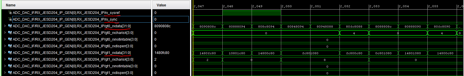
When I set the ADC to send a continuous stream of /K/ characters, the FPGA deasserts sync~ and completes the code group sync phase. When switching back to normal ADC data, the FPGA asserts sync~ again but I don’t see the code group sync or the initial lane alignment sequence in the data coming across. A few important settings that I’m using are :

100 MHz ADC clock
200 MHz FPGA device clock
2 Gbps line rate
LMFK = 2, 2, 2, 32

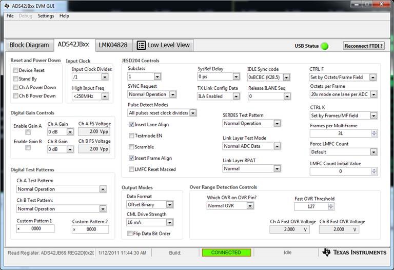
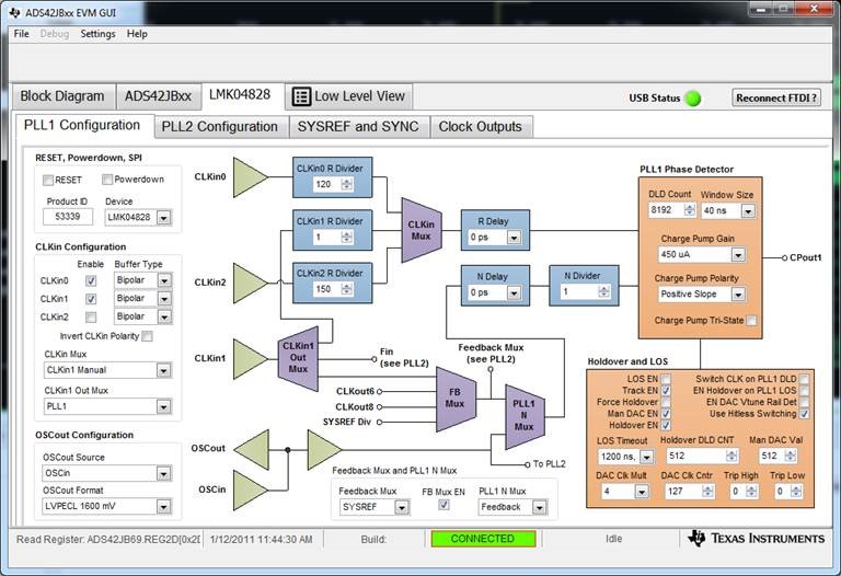
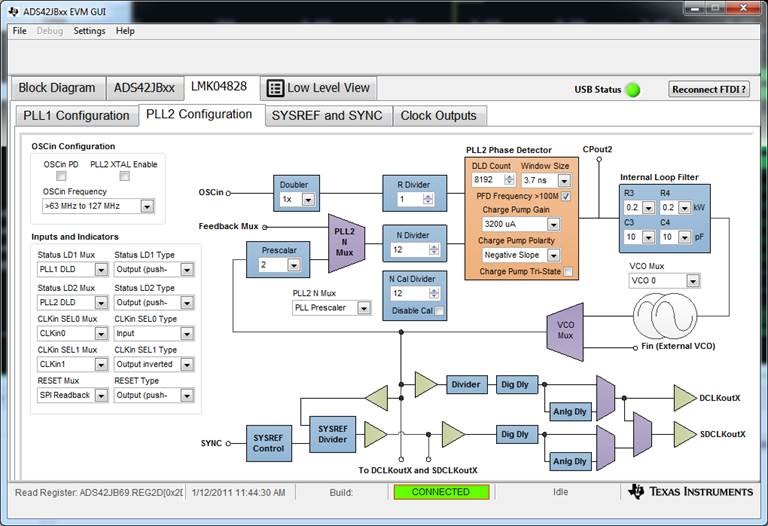
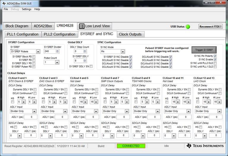
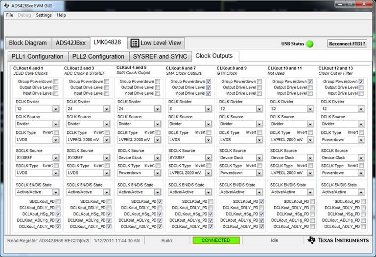
Is there anything obvious that stands out as causing the issue here? For reference, the settings that I’m using in the EVM GUI are below :

Thank you

  • ADS42JB66 100MHz Clk 222 Mode.pptxBranden,

    I got this working with your setup but had to change the SYSREF divider to 768. See attached file. Give this a try.

    Regards,

    Jim

  • Hi Jim, thank you for your response. I tried setting the SYSREF divider to 768 as you suggested but I'm observing the same behavior. Are you able to inspect the decoded 8b10b characters sent over each lane with your setup? What are they when SYNC~ is asserted?
  • Branden,

    I am checking with our firmware team to see if we can setup a signal tap capture of this. Can you verify the ADC register settings you are using match what I have? These values are as follows:

    0x06 0x80
    0x07 0x00
    0x08 0x18
    0x0B 0x00
    0x0C 0x00
    0x0D 0x6C
    0x0F 0x00
    0x10 0x00
    0x11 0x00
    0x12 0x00
    0x13 0x00
    0x1F 0xFF
    0x26 0x06
    0x27 0x03
    0x2B 0x00
    0x2C 0x01
    0x2D 0x13
    0x30 0x20
    0x36 0x00
    0x37 0x00
    0x38 0x00

    Regards,

    Jim

  • Hi Jim,

    Comparing your register settings to mine, the only differences that I found were in register 0x1F which had a value of 0x7F on my end (unused bit in Fast OVR threshold set to 0) and in register 0x2D which was 0x1F (Frames per multiframe set to 31).

    Thanks,

    Branden

  • Branden,

    Here is the ILA data you requested. Did you know the SYNC function on this device is the opposite of what the JESD204B standard calls out? In our system, we invert the SYNC coming out of the FPGA.

    Regards,

    Jim

    ADS42JB46 ILA.zip

  • Hi Jim, thanks for the signaltap data. I did not know that this ADC requires the SYNC to be inverted from the JESD204B standard, glad you pointed that out. After accounting for the inversion in my firmware I am now seeing the link get through the CGS and ILA phases. I was even able to pipe in a tone from a sig gen and see the waveform successfully output by the Xilinx JESD204 IP. Thanks again for your help!