A related question is a question created from another question. When the related question is created, it will be automatically linked to the original question.
If you have a related question, please click the "Ask a related question" button in the top right corner. The newly created question will be automatically linked to this question.
The device is 1MSPS = 1 Mega Samples Per Second, therefor one conversion cycle, to complete one conversion can take 1uS. The digital communications would have to happen within that conversion cycle. The timing diagrams in the datasheet cover the different digital commincation modes available.
Also, if you are interested in learning more about ADC's, we now have an online lecture series, TI Precision Labs-ADCs that can prove helpful.
Thank you for your response I indeed took notice of the lectures and read some of it. But if I understand you correctly it will convert 32-bits a million times per second en not 1 million bits per second, so it is able te send 32 million bits per second.
The reason for my question is that a "sample" is not clearly defined in the datasheet. whether this is 1 or 32-bits.
According to the datasheet the ADS8691 conversion time is 655ns
A sample is one conversion, also could be referred to as a conversion cycle, or one conversion result.
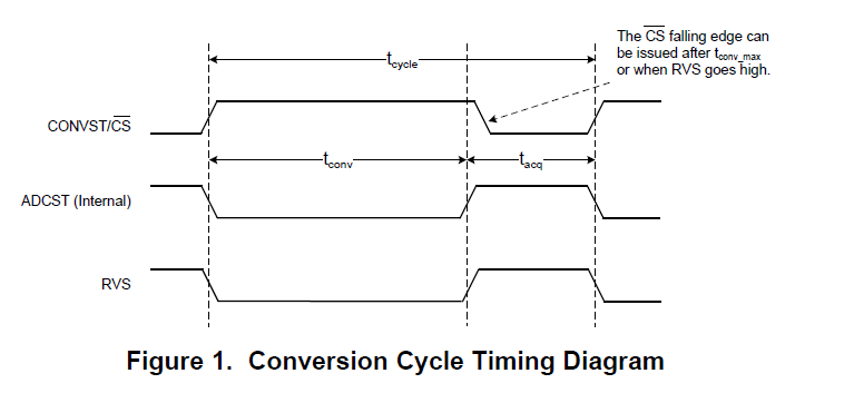
For the ADS8691, Figure1 shows one sample, or, in other words, one conversion cycle, with a time span of t_cycle. The datasheet defines this as a minimum of 1 us. This is where the 1 MSPS comes from, you can get one million samples, AKA conversion results, in one second.
As for the bits, this is something different, and does not necessarily directly connect to the 1MSPS.
Note, in the above picture, the t_cycle, the conversion cycle is divided, this is where the t_conv of 665ns is located, which is part of one conversion cycle.
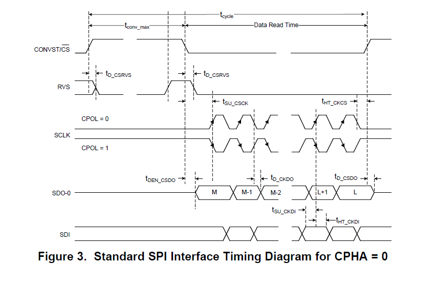
During the data read time is when the bits are transferred, as shown in the figure3 in the datasheet. The output bits follow the SCLK frequency and must be all outputted during the allotted Data Read time, which can be seen is shorter than the t_cycle time.
Thus when you read a sampling rate, this does not refer to the bit output rate.
You will need to check the datasheet based on what interface you are using to be sure to use the correct timing requirements.
There is alot of material available one being TI Precision labs, which is very helpful. I would definitely recommend this as you progress with your design, Section5- SAR ADC Input Drive Design will prove most helpful, I think. Also, TI's Data Converter Learning Center has good information in an overview label broken down into parts, including ADCs.