This thread has been locked.

If you have a related question, please click the "Ask a related question" button in the top right corner. The newly created question will be automatically linked to this question.

DAC121C085: Seperating Grounds with isolator

Part Number: DAC121C085
Other Parts Discussed in Thread: ISO1541,

Hi,

I am trying to get 0-10V analog output. I am using a DAC121C085 and ISO1541. Through a connector i am getting 24v and ground and with the same connector i am sending the analog value.after genereting 0-2.5v with dac i am using an op-amp to make it 0-10V. But as you will notice grounds are seperated so output cant be measured. What can i do for this ?

  • Hello,

    First of all - the feedback network you have designed around U10 will not gain a 2.5V full-scale signal into a 10V output as the circuit you have designed has a gain of 2. You need to modify these resistors in order to achieve the output you desire.

    From the schematic and your question, it sounds like the amplifier is going to drive a load between "Vout" and "GND", where "GND" is also the ground for the isolated side of the ISO1541. Meanwhile the signal chain circuits on the hot-side of the isolation are referred to "AGND", and you therefore want to be able to sense and accommodate for the difference in these grounds. This sort of begs the question - why are you isolating the DAC and amplifier to begin with in this case?

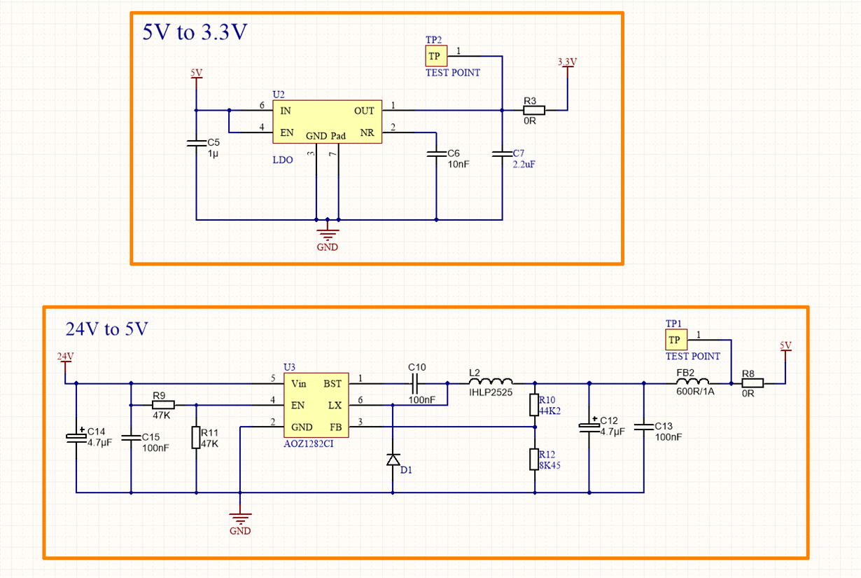
    How are each of these supplies derived from the 24V at the terminal block?

    What is the maximum potential difference between "AGND" and "GND"?
  • I seperated them to reduce noise. I dont know too much about this seperating, i just took an advice and if it is not needed i will remove it.

  • Hello,

    Perhaps the communicated definition of isolation is being confused a bit here.

    One perspective is that I could see someone suggesting isolation from a physical printed circuit board perspective to reduce noise or crosstalk of analog and digital signals. There are variety of opinions on this topic ranging from split ground planes (which ultimately are still connected to one another somewhere on the board), a "star ground" or simply routing signals carefully - being mindful of return paths.

    The other perspective, and what is achieved by a device like the ISO1541, is true electrical isolation via optical, transformer, or capacitive isolation technologies which is typically included for some functional requirement or safety perspective and does not necessarily directly imply reduced noise. If one includes this type of isolation the power supplies are also isolated since circuits on each side of the isolation barrier are referencing a different ground potential. Similarly, the load impedance would be in reference to the "hot side" of the isolation barrier.

    How is the "A3.3V" rail which is used to provide power to the DACs generated? If this isn't an isolated rail, your design will have another functional problem.

    If you do not require electrical isolation as defined in the second paragraph here, then I would suggest you remove the ISO1541 and simply execute proper PCB layout techniques to minimize noise.