


Other Parts Discussed in Thread: THS4141
Conditions of use:
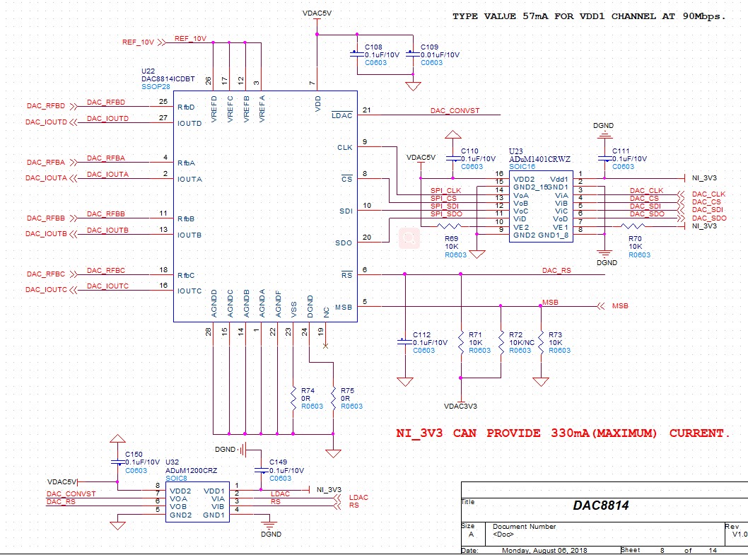
1. SPI control output of DAC8814 through SPARAN6 FPGA of XILINX;
2. DAC88144 channels are used for simultaneous output, of which one channel is converted from single-ended output to differential output.
3. The reference voltage is 10V.
4. The output waveform of the design is amplitude (+10V) and the frequency is 220 KHz square wave.
Schematic diagram:
Principle Diagram of DAC8814 Output Current-to-Voltage Conversion

Principle diagram of DAC8814 output single-ended output to differential output

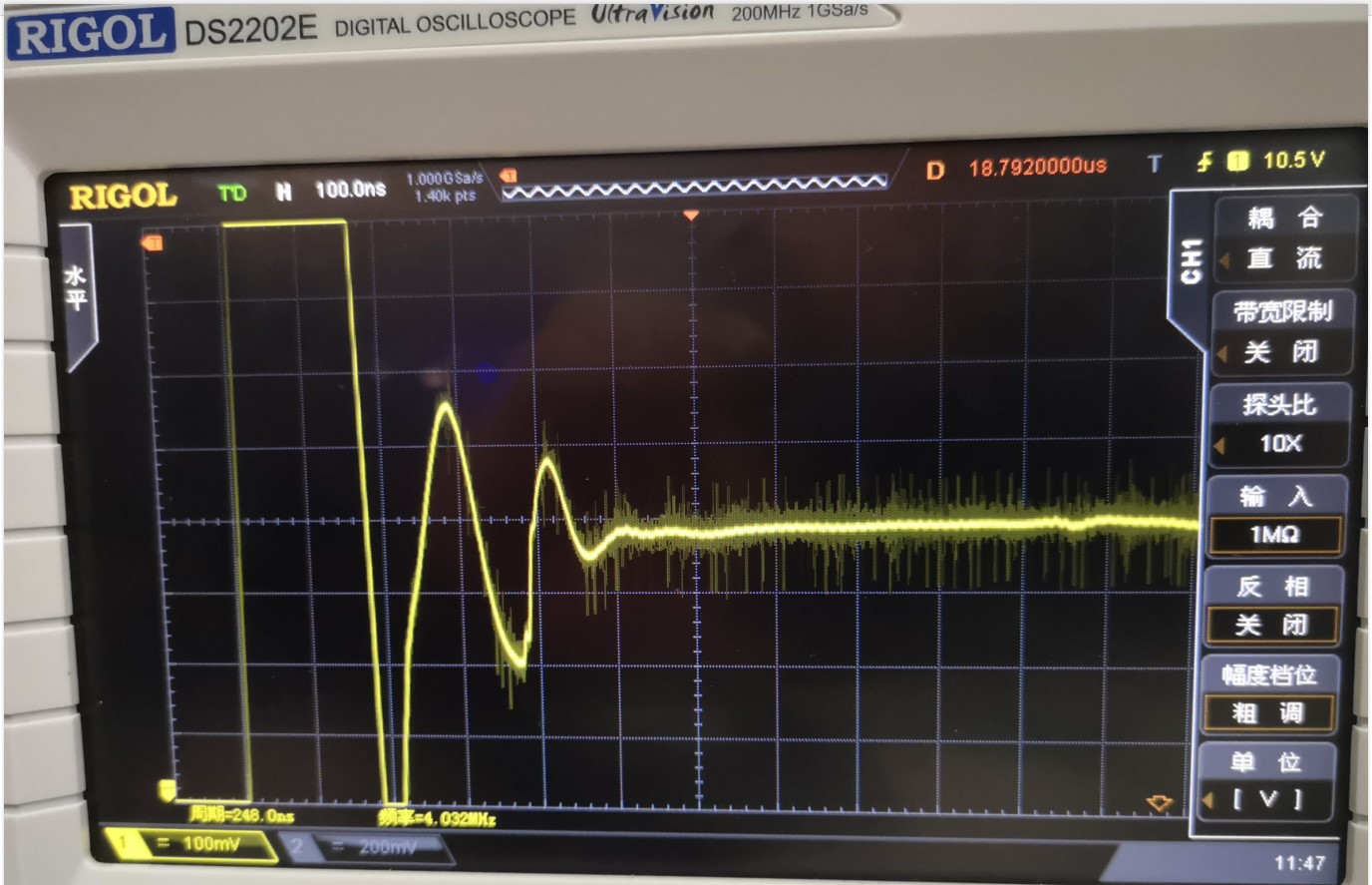
Output waveform measured by oscilloscope:

Debugging problems:
1. When jumping from + 10V to - 10V, or from - 10V to + 10V (full range jump), there is a jitter within 500 ns or so, as shown in the red circle of the above-illustrated wave, and the amplitude is close to 4V.
2. In steady state, the waveform also has a burr of about 200 mV.

