This thread has been locked.

If you have a related question, please click the "Ask a related question" button in the top right corner. The newly created question will be automatically linked to this question.

ADS4245-EP: ADS4245-EP clkout is not proper

Part Number: ADS4245-EP
Other Parts Discussed in Thread: ADS4245, LMK61E2-100M

We have assembled 3 boards with ADS4245-EP. All 3 were working properly.

Now when we checked ADC data was not proper in two cards.

After debugging it is noticed that -

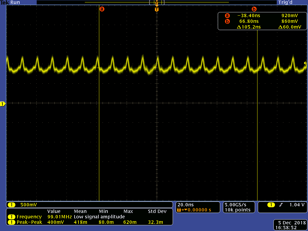
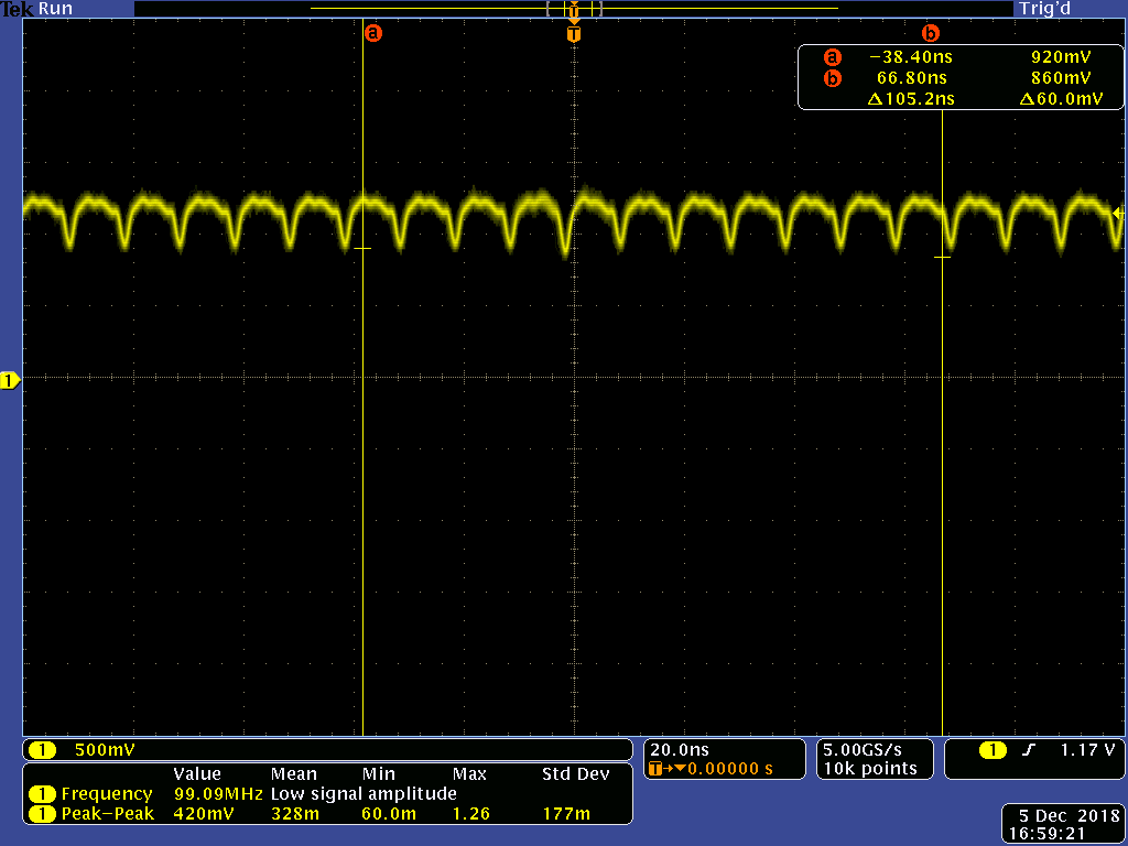
Board1) ADC ADS4245-EP CLKOUT p/n amplitude is not up to expected level  - it is close to 500mVpp (Where as in working card is close to 1Vpp)

Board 2) ADC ADS4245-EP CLKOUT_p is present  - almost 1Vpp whereas CLKOUT_n is not there. (continuity is present between device Pin and monitoring point Via)

I m doubtful If ADC have gone bad.

ALL 3 boards have same clock input. (Probed and Verified)

Kindly comment.

  • Amit,
    The engineer that supports this device is currently out on travel.
    I will see if I can help you in the mean time.
    Can you provide a schematic?
    When you indicate that boards working with ADS4245, you mean the rest of the board? Or did the devices fail after board coming up?

    You currently have 1 working board, and 2 boards not working?
    How is the LVDS clock terminated? Is it double terminated, or single. If double, is LVDS CLKOUT strength set for 50ohm termination?

    What does CLKP/M input schematic look like? It is driven from an LVDS input and ac coupled? When probing, where are you probing?

    Regards,
    Wade
  • All three boards were working, including ADC with complete application code.  
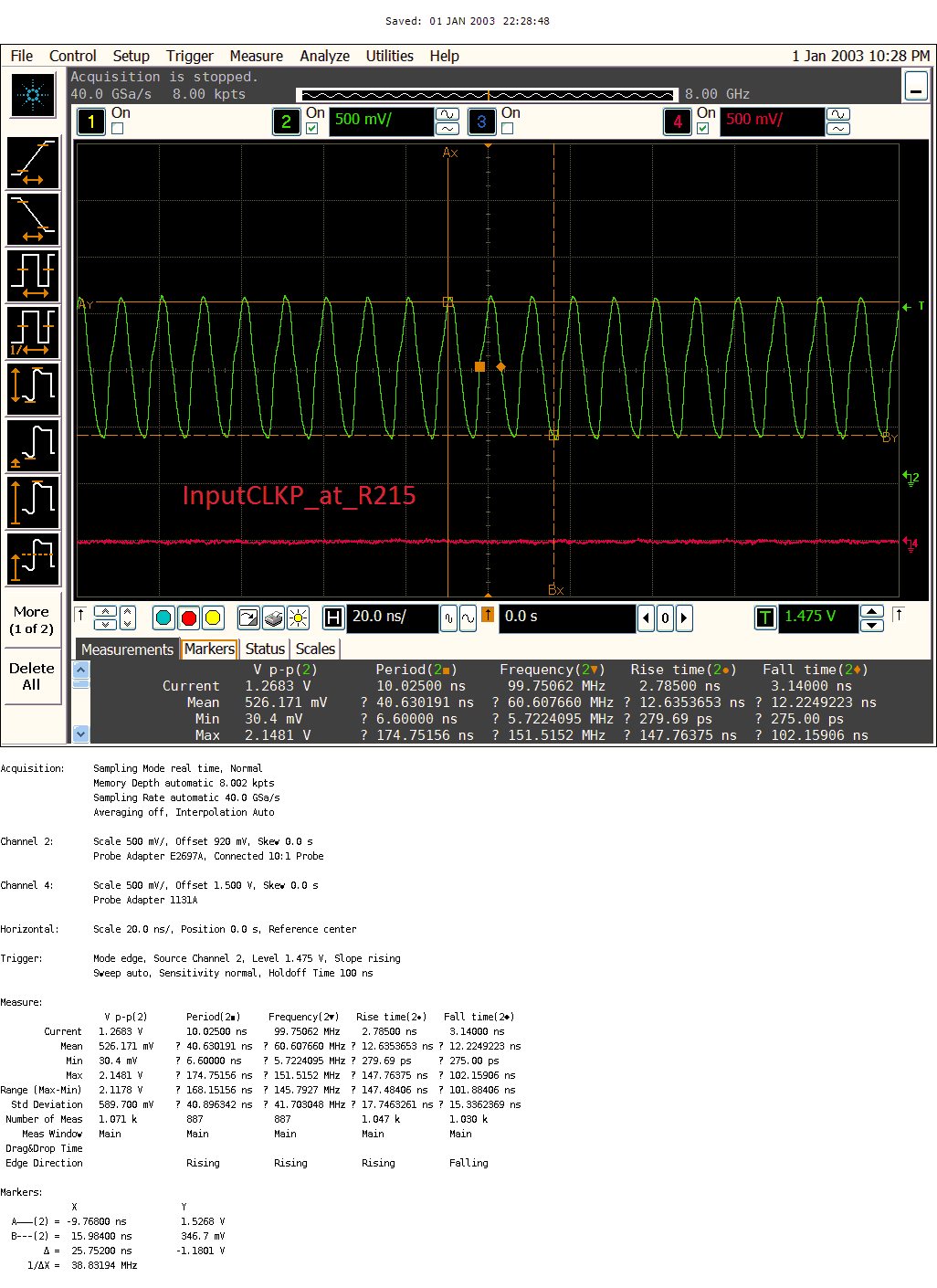
    Input clock is probed at R215 using single ended probe.
    ADC CLKOUT is probed at Via near to ADC on top layer of PCB.
    ADC CLKOUT is connected to single LVDS receiver in FPGA, Internal termination of 100E is Enabled inside FPGA.

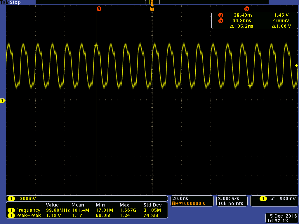
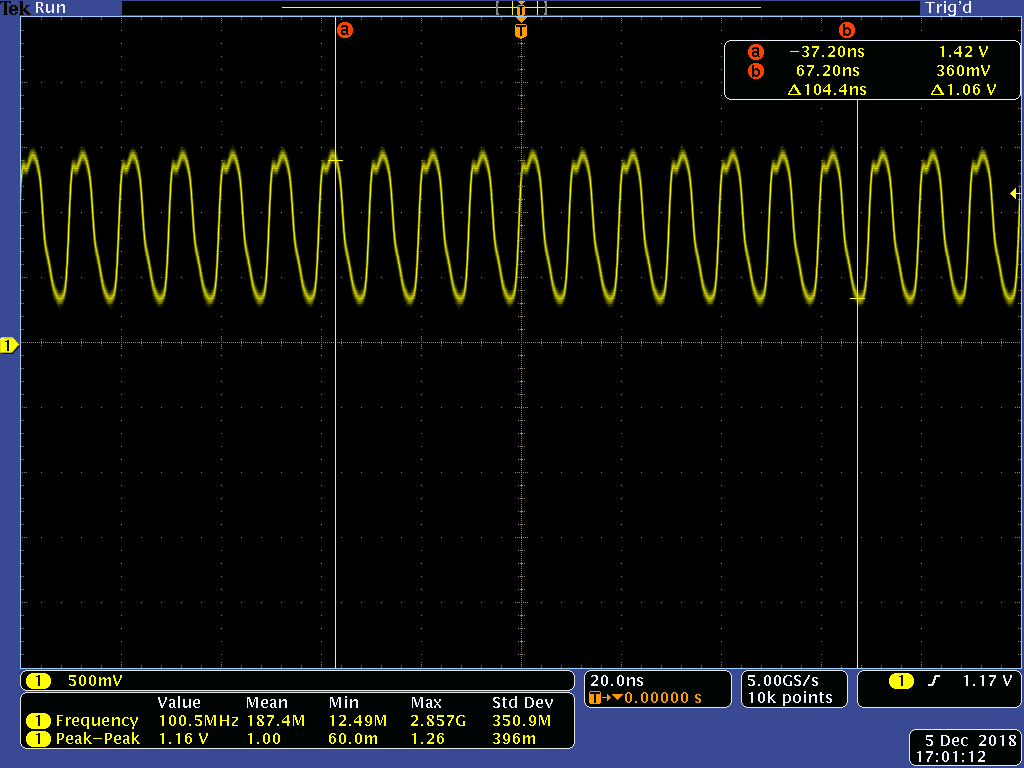
    Images in sequence are :

    1) Board 1 - CLKin (single ended)

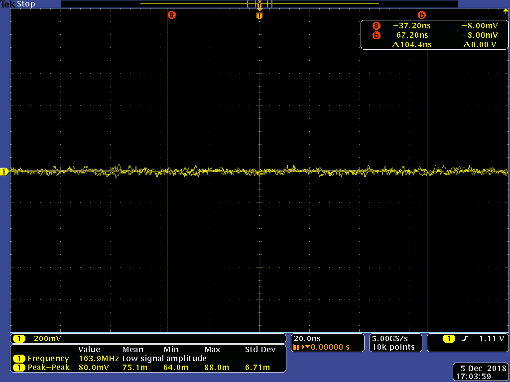
    2) Board 1 - ADC CLKOUTp (Reduced amplitude)

    3) Board 1 - ADC CLKOUTn (Reduced amplitude)

    4) Board 2 - CLKin_p (single ended)

    5) Board 2 - ADC CLKOUTp (Present -  approx 1Vpp)

    6) Board 2 - ADC CLKOUTn (NOT Present )

    7) Board showing probing locations

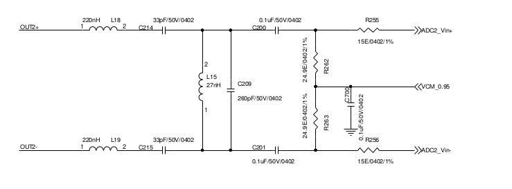
    8) Last two images  - Schematic

  • Your input clock does not look correct.
    Your input clock is showing a single ended swing of 400mV, about the correct common mode of ~1V. It shoudl have 800mV single ended swing for LVPECL.
    What is the device that is driving the clock? I could not find it with search.
    Can you provide this? Possibly Rbias (R221, R222) needs adjusting to increase output swing.
    This app note covers some of this detail. It will depend on what VCC is used.
    www.ti.com/lit/an/scaa056/scaa056.pdf
    Look at section 2.2

    Regards,
    Wade
  • In the attached images input clock is approx 1Vpp for Single ended....

    Also, with the same input clock the board was working from 3 Months.

    Well I will go through the ADS4245-EP input clock requirement....

  • Amit, I apologize. I read the marker as the delta measurement.

    Can you tell me what device is driving the clock? There is note that it was switched from the SI571.

    Also, the VCM output goes to an off-sheet connector. What is connected to the VCM output? There is other e2e post that indicates there may be relationship of having load on VCM to cause startup issues with clock.

    Regards,
    Wade
  • The clock source what we used is L0M0KM6010E32IA, 100MHz, LVPECL .

    The VCM is connected to output of AC coupled filter output to provide VCM raised inputs to ADC.

    Schematic is below.

    Kindly comment.

  • With this inputs can we confirm that ADC is not functioning, as CLKOUT is not proper.

    Shall I go for replacing the ADC chip.

    Any other point to check which may confirm that ADC is not functioning properly.

    Kindly comment.

  • Amit,
    I do not see any issues with your schematic. Though it is very unusual that you would have 2 devices fail to operate correctly in such a similar way without there being a symptomatic issue.
    I would suggest replacing devices, and evaluate.

    The engineer that supports this device is back in the office soon. He may be able to add some additional insight.
    Regards,
    Wade
  • Hi Amit,

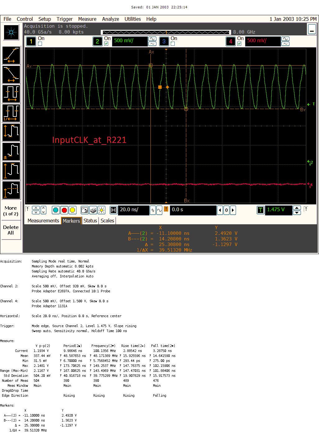
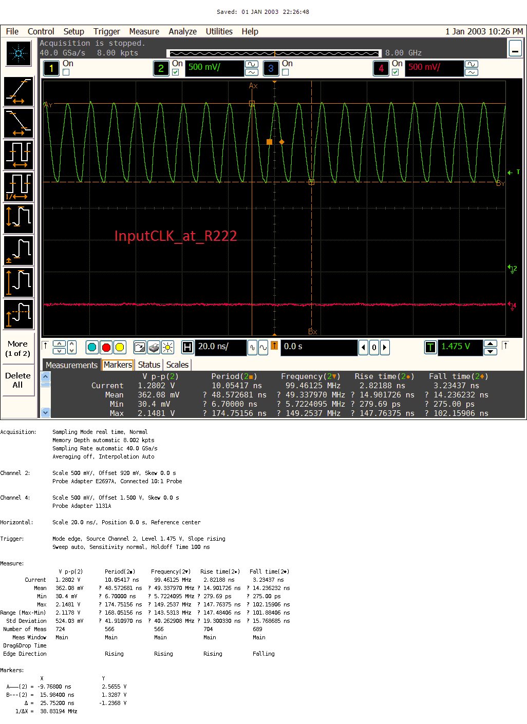
    Could you show scope shots of the input clock at R221 and R222 and both sides of R215 on a good board and a bad board. The scope shots only show one side of R215 and do not show the output of the clock source before AC coupling into the ADC.

    Thanks
    Christian
  • I will capture and post the same today...

  • HI,

    I replaced the ADC in one of the board. Whereas after replacing ADC the situation is same. ADC_CLKOUTp is ok and ADC_CLKOUTn is with reduced amplitude.

    I have captured waveforms of Input clock at R221, R222 and at R215. These waveforms looks OK. Kindly Check.

    Regards,

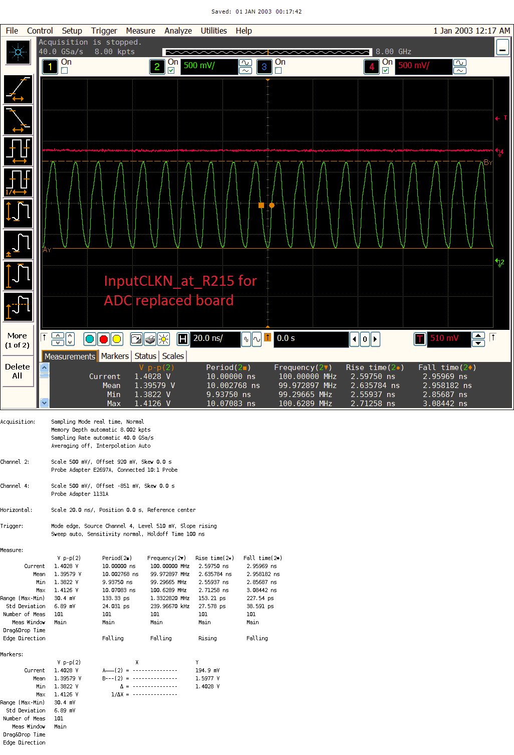
  • Looking at the new scope plots I see the following Input clock levels at the input pins of the DUT:

    Before replacing ADC:
    ADC_CLKINP at R215 at DUT pin: 0.3467V to 1.5268V (1.1801Vpp-se)
    ADC_CLKINN at R215 at DUT pin: 0.3231V to 1.5014V (1.1784Vpp-se)
    ADC_CLKIN = 2.3585Vpp-diff

    After replacing ADC:
    ADC_CLKINP at R215 at DUT pin: 0.1754V to 1.5565V (1.3811Vpp-se)
    ADC_CLKINN at R215 at DUT pin: 0.1949V to 1.5977V (1.4028Vpp-se)
    ADC_CLKIN = 2.7839Vpp-diff

    This is a very high clock level for a 1.8V device. Typical LVPECL levels are on the order of 0.5-0.8Vpp-se. All specifications and typical plots in the datasheet were taken with a 1.5Vpp-diff clock at the input. I suspect the large input swing is squeezing the bias current source at the input buffer and corrupting the input clock internally. Can you please try to reduce the input clock so for a nominal level of 1.5Vpp-diff?

    Regards,
  • I will Check and update you....

  • Related to LVPECL clock following are the details from datasheets:

    1) LMK61E2-100M Datasheet: LVPCEL clock

        VOD Output Voltage Swing  = 700(min) 800(typ) 1200(Max) mV

        VOUT_DIFF_Vpp Differential Output Peak-to-Peak =  2x|VOD|

        From this Vdiff can be 2.4Vpp

    2) ADS4245-EP

      CLKP, CLKM Input applied to the terminal: Max AVDD(1.8V)+0.3V = 2.1V

    As you wrote the ADC plots are wrt 1.5V differential clock and ADCCLK in of 2.3585Vpp and 2.7839Vpp is not suitable for 1.8V device.

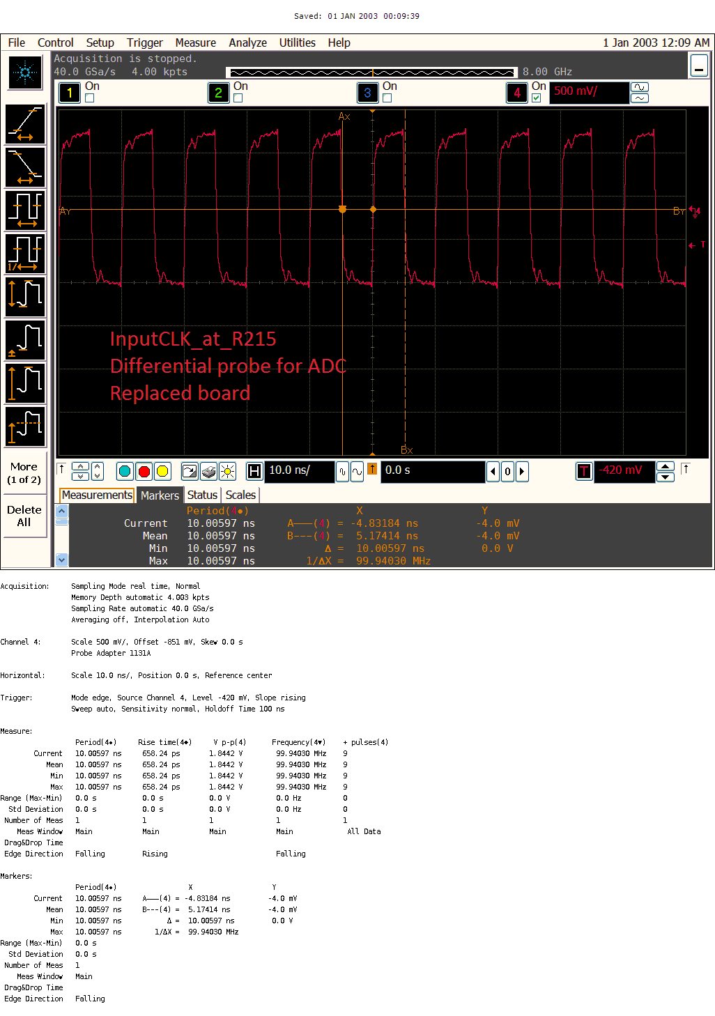
    For this Pls Check Input clk probed with differentail probe which was showing Vpp of 1.8442V

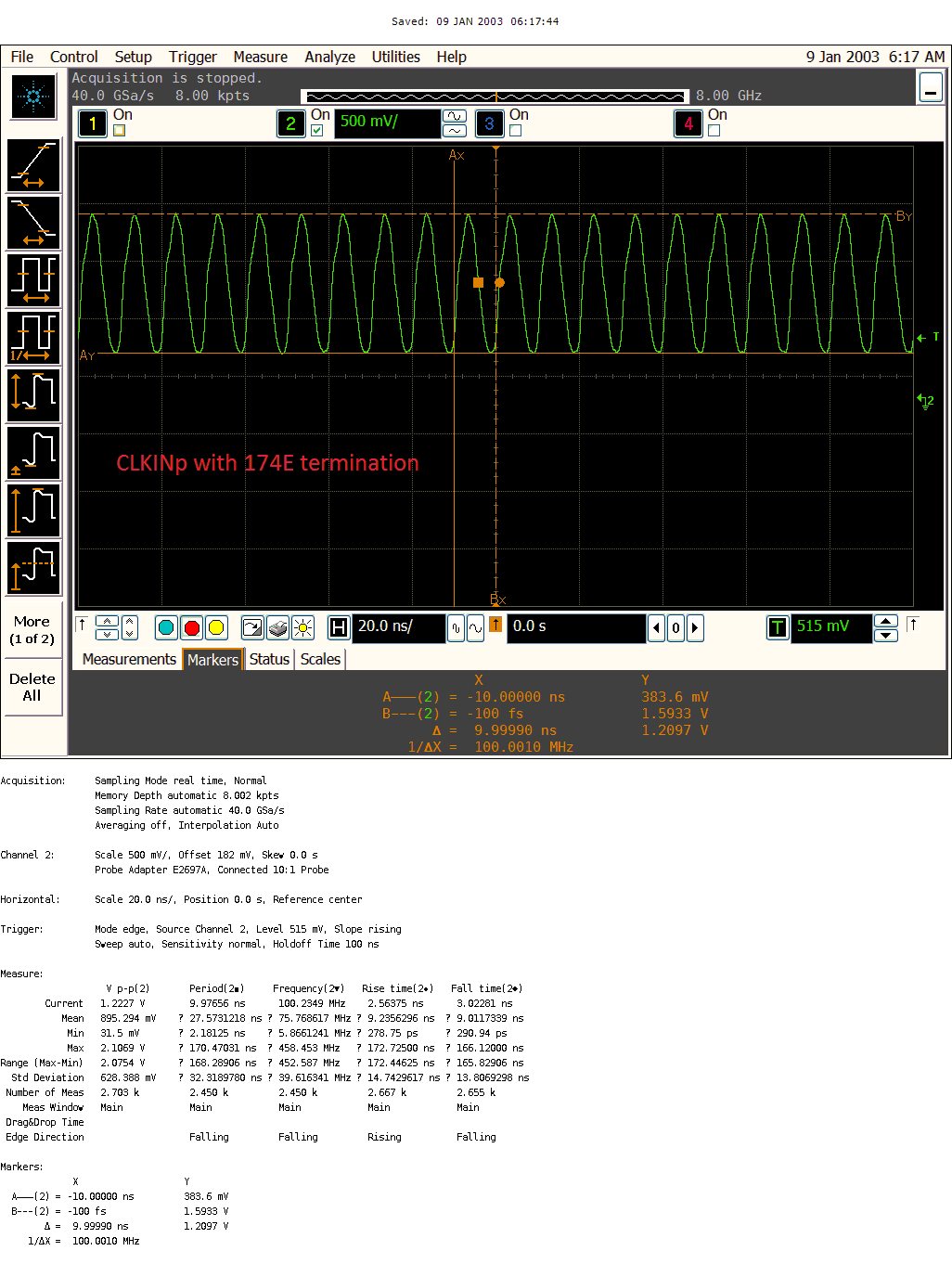
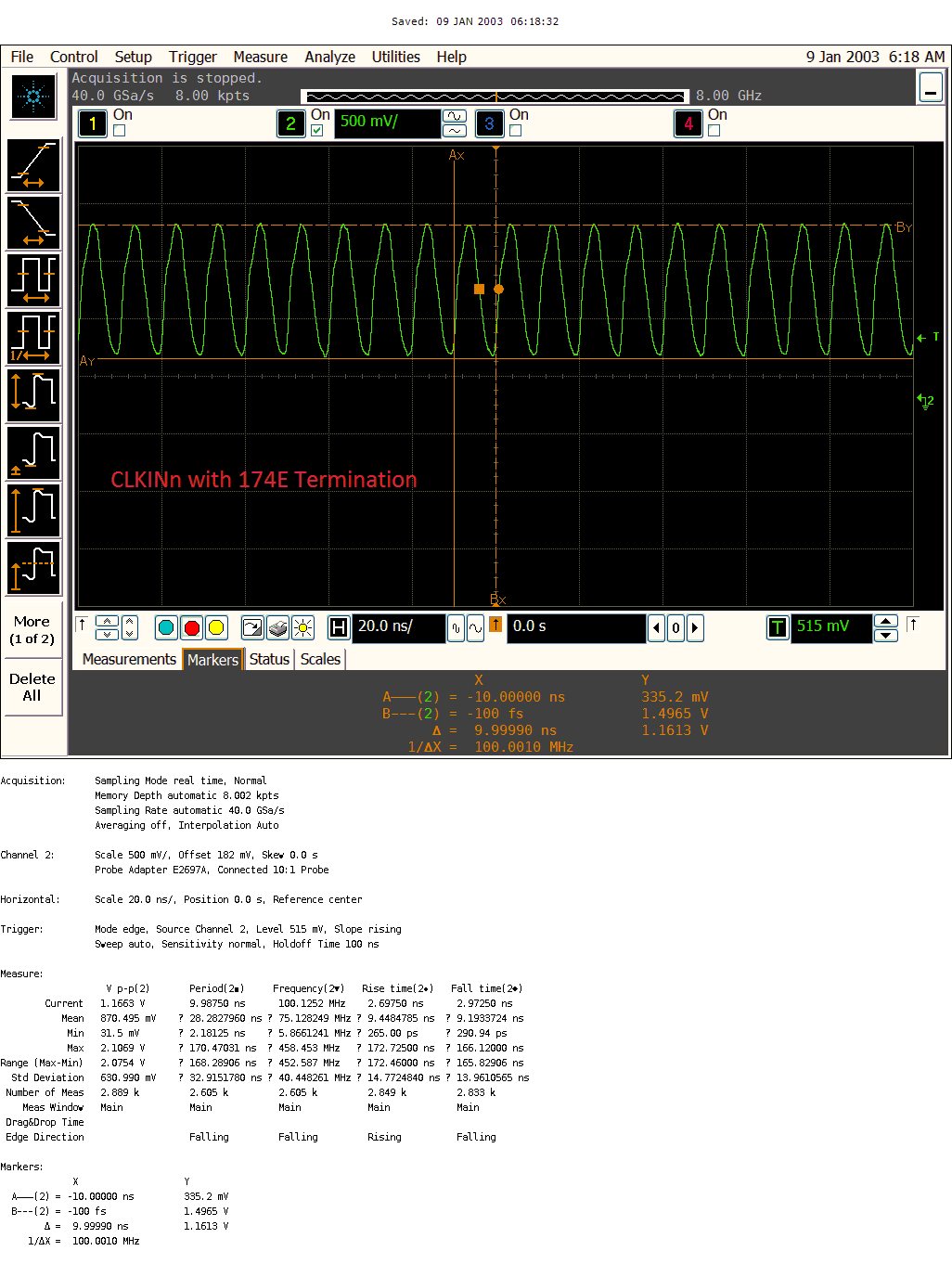
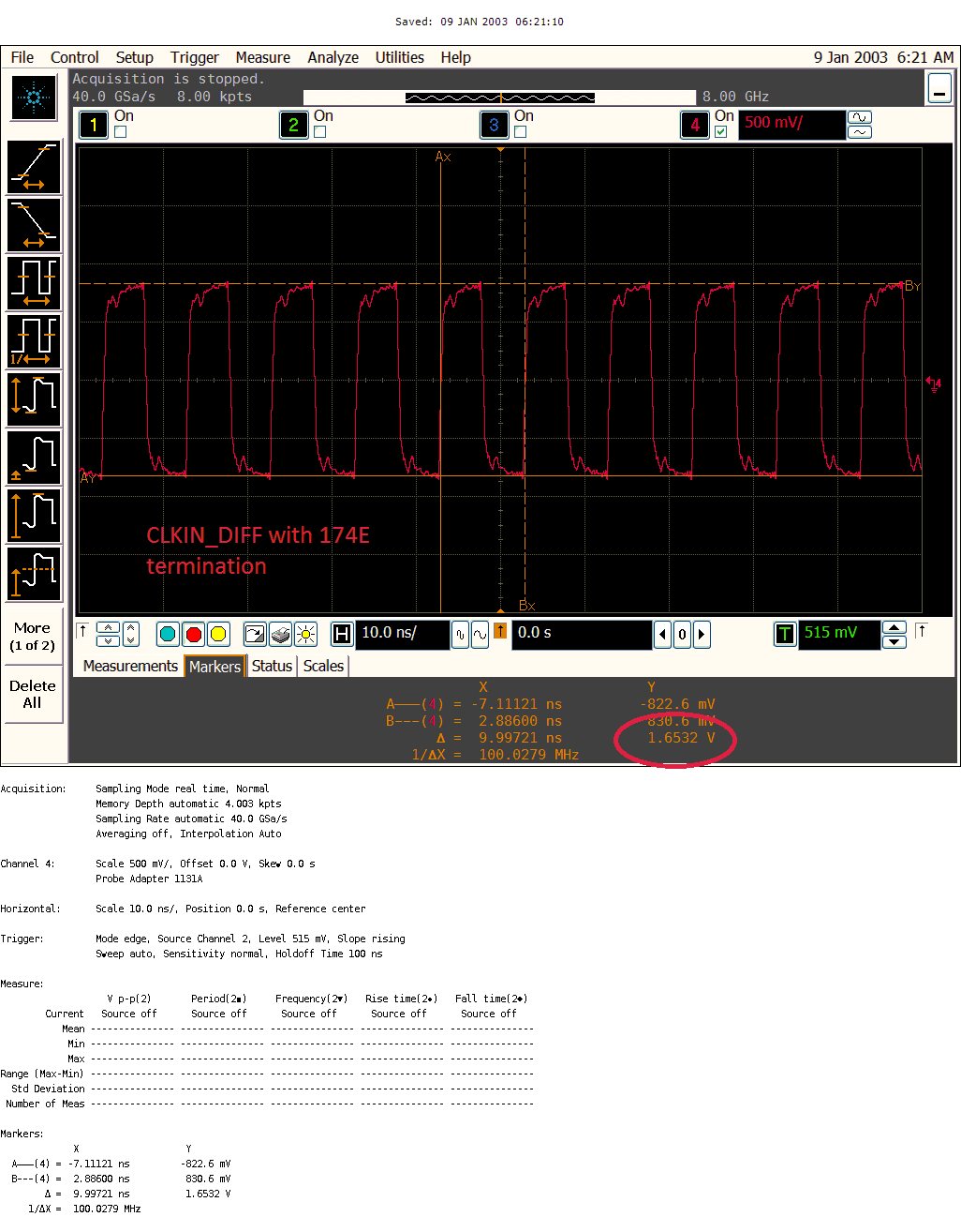
    In order to reduce the swing for input clock, the input 150E termination is replaced by 174E which is giving Vpp of 1.6532Vpp.

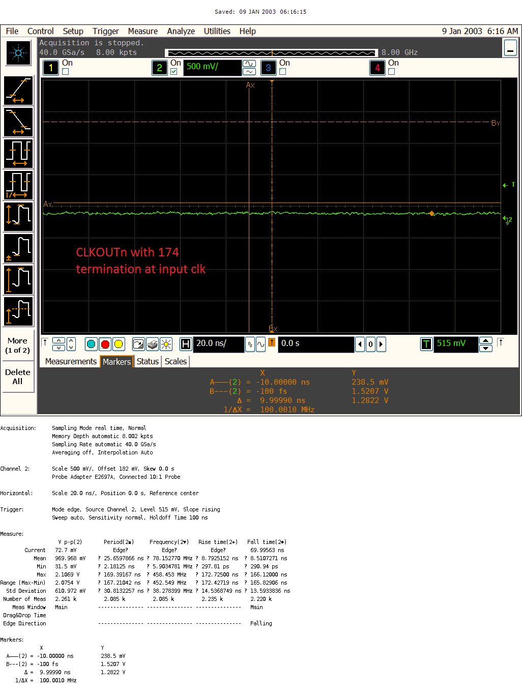
    With this change the is no improvement found in the clk out of ADC.

    Still CLKp is present with 100MHz and CLkn is absent.

    Other Input and output clocks probed are attached for your reference.

    Kindly comment on this.

  • Hi Christian,
    Please help to share your comments.
  • Hi,

    Regarding the LMK61E2-100M specs, I agree the datasheet calls for 2.4Vpp-diff output signal, however, this device is powered by 3.3V. The ADC receiving this signal is powered by 1.8V. It is my recommendation to lower the input clock signal swing to a nominal value of 1.5Vpp-diff to be in line with the ADC specs and characterization.

    Regarding your comment “CLKP, CLKM Input applied to the terminal: Max AVDD(1.8V)+0.3V = 2.1V”, this is an absolute maximum spec which must be respected to avoid catastrophic damage/failure of the device. This spec should not be interpreted as the max clock level under which the device will meet datasheet specs or even function normally. It is only the level by which damage to the device is avoided.

    This leads to a question about starting up your system. Does the ADC ever receive the input clock before the ADC is provided power? If so, this is a violation of the absolute max spec and could be causing problems. Please confirm that the system power up sequence avoids this situation.

    Regarding the new screen shots provided, I need clarification from you. The plots show the following values:

    Plot1: CLKinp => 0.3836V - 1.5933V => 1.2097 Vpp-s.e.
    Plot2: CLKinn => 0.3352V - 1.4965V => 1.1613 Vpp-s.e.
    Plot3: CLKindiff => 1.6532Vpp-diff

    Taking the difference of plots 1 and 2 yields 2.371Vpp-diff and does not agree with plot 3 showing 1.6532Vpp-diff. Could you clarify. Seems the input signal still might be very high.

    Thanks
    Christian
  • HI,

    I totally agree with your comments for "“CLKP, CLKM Input applied to the terminal: Max AVDD(1.8V)+0.3V = 2.1V".

    I need to check the power up sequence to confirm whether ADC clock is present before ADC power up. I will do it.

    Mean while for LMK61E2-100M 3.3V and ADC 1.8V device, can you pls tell me what type of termination and value is suitable for clock input instead of 150E.

    Also I need to know new clock source part number suitable for ADC, for next version of schematic.

    Regarding waveform plots...Plot 3 is captured with Differential probe (and I felt it is correct)... I don’t have better clarification for this, pls let me know how to capture

    proper single ended and differential waveform for the clock.

    One more logical doubt is that "Even though LMK is powered with 3.3V and it supports LVPECL clock output, then the clock swing should be as per standard LVPECL signal levels irrespective of the Power of the device". Kindly comment on this.

    Regards,

  • Hi Again,

    For the scope captures, please confirm that the scope input impedance is set to high impedance for both measurements. The differential measurement should align with the single-ended measurements.

    Also, the LVPECL termination changed from 150ohms to 174ohms. For a fixed bias current, this will increase the clock drive and not decrease the clock drive. Could you please try changing the output termination of the LMK device to 100ohms and probe signals at LMK output and ADC input.

    Finally, your initial thread post stated you had 3 ADC EVMs, all of which were initially working but two that began showing failures. Is the one EVM that remained functional when you reported the issue still showing proper operation? If so, are you able to swap devices between functional and non-functional EVMs in an effort to discern if the DUT is the issue or the EVM on which it resides? If you are able to do this experiment I recommend retaking scope captures of LMKOUT and ADC CLKIN and CLKOUT of both EVMs before and after the swap.

    Thanks
    Christian
  • HI,

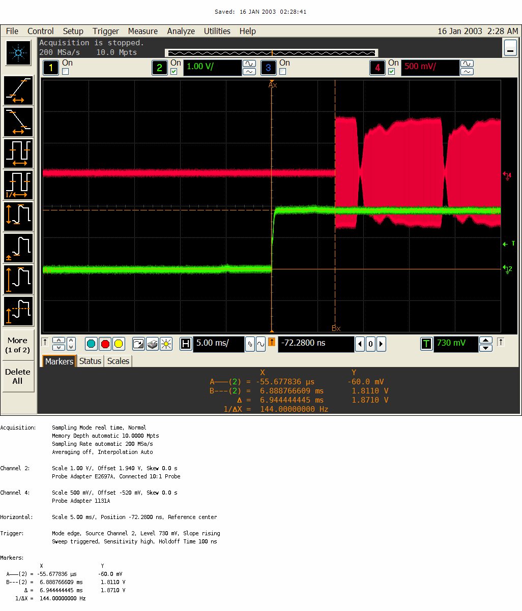
    as you wrote in last post, I check the power sequence for clock and the ADC. The ADC power 1.8V is almost 7 ms earlier compared to clock to be present for ADC.

    Pls check the Plot below.

    As you said I will confirm the probe impedance for both.

    I will upload the Plots with 100E termination on clk.

    Regarding boards,

    Even the third board which was working, now have same status.

    The details are :

    Board 1 and Board 2 - ADC output clk   - CLKOUTp is present "100MHz", CLKOUTn - "Not present"

                                            Even then some how (may be as I am using differential LVDS receiver buffer inside FPGA), I am getting clk inside FPGA. because of which a function test is passing at present.

                                            But Note that still CLKOUTn is not present on Board 1 and Board 2.

    Board 3:         Both ADC CLK p & n are continuously changing. they are not stable at 100 MHz.

    Kindly comment.

  • The power sequence looks OK.  I still recommend to attempt to target a nominal input clock swing of 1.5Vpp-diff to match the ADC datasheet nominal value.  

    At this point, I suspect the termination or configuration in the FPGA might not be correct.   I recommend removing the FPGA load from the CLKOUT (open this path) and terminate (100ohms-diff) near the ADC and probe here to determine if ADC CLKOUT is functioning properly.

    Thanks

    Christian

  • HI,

    As you suspect on FPGA termination, I also suspected on this and following things I tried to check this...

    1) Removed FPGA On chip termination of 100E and provided it on PCB near to ADC physically.

       -  NO improvement found in CLK outputs

    2) (Then I thought may be clk site in FPGA has gone bad) Thus wired same clock outs to some other differential clock site (pins) in FPGA  and disabled the old site connection (Physically track was present. In order to isolate completely from old clk site I have to cut the track and I dont want to do it now..).

     -  NO improvement found in CLK outputs

    Regards,