Other Parts Discussed in Thread: , AFE58JD32
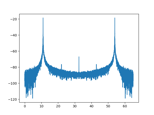
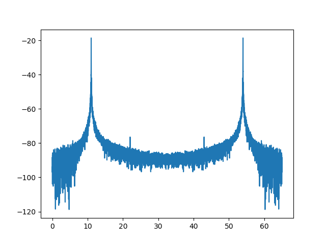
I am seeing a large spur at fs/2 due to each channel having an odd and even sampler. It seems that the dc offset for each is slightly different. I can remove the fs/2 spur in postprocessing by using the following code before an fft
idata[0::2] = idata[0::2]-np.mean(idata[0::2]) (remove offset on even data)
idata[1::2] = idata[1::2]-np.mean(idata[1::2]) (remove offset on odd data)
then an fft of idata works as expected and there is no fs/2 spur.
I want to be able to remove the offset in the adc but on page 61 of the datasheet it says that
"These two register controls are duplicated in the Register Maps section and indicated as the OFFSET_CHx control because the same offset
must be subtracted from both the odd and even data stream."
On page 131 of the datasheet there are two registers for OFFSET_CH1 but it says to enter the same value from both.
Is there a way to correct the offset for odd and even values independently?