This thread has been locked.

If you have a related question, please click the "Ask a related question" button in the top right corner. The newly created question will be automatically linked to this question.

ADC12DJ3200: ADC12dj3200 calibration and SNR

Part Number: ADC12DJ3200

HI,

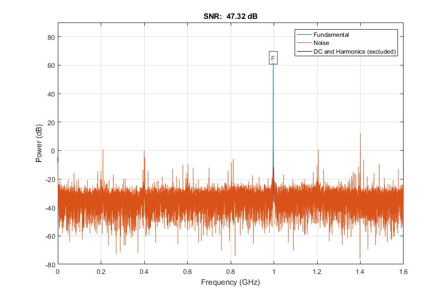
I am using a adc12dj3200 in jmode=3 (dual channel), and using a single channel only at sampling 3200 MHz.

I am trying to improve the SNR via background calibration and offset calibration for continuous operation.

With my best effort I am seeing 47dB SNR. (without offset cal (muting, then background cal enabled I see 30-40dB SNR).

1 - Since I am using one channel , is it possible to dedicate the core C to only service Core A, and not Core B? to

   get a better SNR? (would it help?)

  Thanks,

Shervin

  • Hi Shervin
    If you will always only need a single ADC channel you could power down the unused ADC-B channel. This can be done by setting PD_BCH in register address 0x209h. Please note this should not be done if you do plan to use the B channel at any time. See the NOTE which precedes table 6.4 for more details on the implications of powering down the output serializers.
    If your application has a narrow environmental temperature range you may get slightly better performance using Foreground Calibration mode only, with Foreground Offset Calibration enabled.
    Additional circuitry is required when using Background Calibration and the device performance can be slightly worse in this mode compared with Foreground Calibration mode.
    Best regards,
    Jim B
  • Hi Jim,

    I am seeing around 5 dB better SNR, when using Bg calibration vs Fg calibration.

    Also as I read the datasheet, Foreground Offset calibration is only enabled/applicable when the adc input is muted.

    When running, the Foregroung offset calibration is disabled and Foreground calibration is enabled and triggered at some time,

    followed by the acquisition. (hoping that the conditions remain the same).

    Can someone look into this, as even 47 dB is not going to help me.

    Thanks,

    Shervin 

  • Hi Shervin
    What is the frequency of the signal you are capturing? What is the power you are setting it to in dBFS?
    I will try to test using similar settings and signal tomorrow to see if I can provide any guidance on getting better performance.
    Best regards,
    Jim B
  • Hi,

    Looking at page 19 of the adc12dj3200 datasheet, it is indicated that background calibration is used by TI test and  a large 

    signal. I am not sure what the Ain=-1dBFs means without mention of a balun loss, if a balun is used or not. ( 3 dB is typical)

    I am using a 997 MHz signal at 4dBm into the adc ( going through a balun). The adc input range is at default (800mV pp) and sees a signal 

    at +/-1800 counts, -1.1dBFs

    I am also calculating SNR by removing HD2-9 and DC.

    I am trying to narrow down if this is a system design related.

    Thanks,

    Shervin

  • Hi Shervin
    -1dBFS means 1 dB below the ADC full scale signal range, ie. 1dB below the beginning of clipping of the sine wave signal. The production test setup will adjust the generator output to achieve the power level noted in the datasheet for that test.
    The actual signal level at the generator depends on the insertion loss of the various cables, filters, baluns, etc. used in the setup.
    Best regards,
    Jim B
  • This means that my test case agrees with the TI setup in the datasheet. What you have mentioned is the obvious.

    My question was to inform you how I interpreted the datasheet.

    Your previous email indicated you will look into the measurement with your setup.

    I am still waiting

    Shervin

  • Hi Shervin

    I gathered data at 3200MSPS in JMODE3 with 997.77MHz input frequency. The results are in the attachment below:

    ADC12DJ3200 JMODE3 3200MSPS 997MHz Fin.pdf

    I used foreground calibration mode with offset calibration enabled in the first plot. The second plot uses background calibration with background offset calibration enabled. 

    Please compare these plots with the results you are getting. If you can identify the limiting harmonics or spurs that will help determine what the problem may be. 

    If you can share the register settings you are using along with an FFT plot of our results I can review them as well.

    Best regards,

    Jim B

  • siggen_997MHz_4dBm_PFR_locked_1-4GHz_LP_filter_MINI-CIRCUITS-VLF-1450+_BgCalEn_BgOoffsetCalDis_BgOffsetFiltDis_a.txtHi Jim,

    Thanks for looking into this. Looking at your results, I see :

    analysis windows samples   =65536

    RBW                                               = 48828 Hz

    tone freq                                     = 997.77 MHz

    window                                      = blackman

    For analysis I am using

    analysis windows samples   =65536

    RBW                                               = 48828 Hz

    tone freq                                     = 997 MHz

    window                                      = kaiser

    -Are you choosing the tone freq to fall on a bin?

    -I am guessing you are storing samples, and post analyze the data.

    what type of processing are you using to arrive at SNR?

    I am attaching my adc data ( ascii format), setting, spectrum plot  and it is 81920 points long, and you can choose 65536 points for analysis.

    the background cal related setting is set manually after temperature stablizes, where I mute the input, cal the offset, then disable the

    offset, and run in bg cal.

    Thank,

    Shervin

    0x0000,       0x30,
    0x0002,       0x00,
    0x0003,       0x03,
    0x0004,       0x20,
    0x0005,       0x00,
    0x0006,       0x05,
    0x000C,       0x51,
    0x000D,       0x04,
    0x0010,       0x00,
    0x0029,       0x20,
    0x0029,       0x60,
    0x002A,       0x00,
    0x002C,       0x00,
    0x002D,       0x00,
    0x002E,       0x00,
    0x0030,       0xC4,
    0x0031,       0xA4,
    0x0032,       0xC4,
    0x0033,       0xA4,
    0x0038,       0x00,
    0x003B,       0x00,
    0x0048,       0x00,
    0x0060,       0x01,
    0x0061,       0x01,
    0x0062,       0x01,
    0x0063,       0x00,
    0x006B,       0x00,
    0x006C,       0x01,
    0x0070,       0x01,
    0x0071,       0x00,
    0x007A,       0x00,
    0x007B,       0x00,
    0x007C,       0x00,
    0x007E,       0x00,
    0x007F,       0x00,
    0x0080,       0x00,
    0x0081,       0x00,
    0x0082,       0x00,
    0x0083,       0x00,
    0x0084,       0x00,
    0x0085,       0x00,
    0x0086,       0x00,
    0x0087,       0x00,
    0x0088,       0x00,
    0x0089,       0x00,
    0x008A,       0x00,
    0x008B,       0x00,
    0x008C,       0x00,
    0x008D,       0x00,
    0x008E,       0x00,
    0x008F,       0x00,
    0x0090,       0x00,
    0x0091,       0x00,
    0x0092,       0x00,
    0x0093,       0x00,
    0x0094,       0x00,
    0x0095,       0x00,
    0x0102,       0x00,
    0x0103,       0x00,
    0x0112,       0x00,
    0x0113,       0x00,
    0x0122,       0x00,
    0x0123,       0x00,
    0x0132,       0x00,
    0x0133,       0x00,
    0x0142,       0x00,
    0x0143,       0x00,
    0x0152,       0x00,
    0x0153,       0x00,
    0x0160,       0x00,
    0x0200,       0x00,
    0x0061,       0x00,
    0x0201,       0x03,
    0x0202,       0x1F,
    0x0203,       0x01,
    0x0204,       0x02,
    0x0205,       0x00,
    0x0206,       0x00,
    0x0207,       0x00,
    0x0208,       0x00,
    0x0209,       0x00,
    0x0061,       0x01,
    0x0000,       0, 10
    0x0200,       0x01,
    0x0210,       0x00,
    0x0211,       0xF2,
    0x0212,       0xAB,
    0x0213,       0x07,
    0x0214,       0x01,
    0x0215,       0x00,
    0x0216,       0x02,
    0x0217,       0x00,
    0x0218,       0x00,
    0x0219,       0x02,
    0x0220,       0x00,
    0x0221,       0x00,
    0x0222,       0x00,
    0x0223,       0x10,
    0x0224,       0x00,
    0x0225,       0x00,
    0x0228,       0x00,
    0x0229,       0x00,
    0x022A,       0x00,
    0x022B,       0x20,
    0x022C,       0x00,
    0x022D,       0x00,
    0x0230,       0x00,
    0x0231,       0x00,
    0x0232,       0x00,
    0x0233,       0x40,
    0x0234,       0x00,
    0x0235,       0x00,
    0x0238,       0x00,
    0x0239,       0x00,
    0x023A,       0x00,
    0x023B,       0x80,
    0x023C,       0x00,
    0x023D,       0x00,
    0x0240,       0x00,
    0x0241,       0x00,
    0x0242,       0x00,
    0x0243,       0x10,
    0x0244,       0x00,
    0x0245,       0x00,
    0x0248,       0x00,
    0x0249,       0x00,
    0x024A,       0x00,
    0x024B,       0x20,
    0x024C,       0x00,
    0x024D,       0x00,
    0x0250,       0x00,
    0x0251,       0x00,
    0x0252,       0x00,
    0x0253,       0x40,
    0x0254,       0x00,
    0x0255,       0x00,
    0x0258,       0x00,
    0x0259,       0x00,
    0x025A,       0x00,
    0x025B,       0x80,
    0x025C,       0x00,
    0x025D,       0x00,
    0x0297,       0x00,
    0x02B0,       0x00,
    0x02B1,       0x05,
    0x02B2,       0x00,
    0x02B3,       0x00,
    0x02B4,       0x00,
    0x02B5,       0x00,
    0x02B6,       0x00,
    0x02B7,       0x00,
    0x02C0,       0x00,
    0x02C1,       0x1F,
    0x02C2,       0x00,

  • Hi Shervin

    I imported your data to High Speed Data Converter Pro so I could do equivalent processing.

    The attached file has the original information plus several slides showing your data using standard performance calculations, and a few with specific tones notched out.

    ADC12DJ3200 JMODE3 3200MSPS 997MHz Fin with customer data.pdf

    What I see in your results are some spurs that I don't expect to be that high, along with worse than expected HD2-HD5 performance.

    I would recommend double checking that none of these spurs are present in the input signal applied to the ADC, or at frequencies that could alias back into the ADC spectrum. I would look at the applied signal using a spectrum analyzer with a span from 0 Hz to at least 8 GHz. 

    If you are not already doing so, please add a bandpass filter into the signal path to ensure only the intended signal is applied. If bandpass filters are not available then a lowpass filter can also be used.

    If the input signal is already clean I would then look to any possible noise coupling onto the ADC clock or power nets or potential ADC setup issues.

    If the ADC is on a board of your design I would like to review the register setting/sequence being used, and the schematic if that can be shared.

    I hope this is helpful.

    Best regards,

    Jim B

  • Hi Jim,
    Thank you for looking at my data.
    As you suggested I am using a Low Pass filter MINI-CIRCUITS-VLF-1450+ before the ADC.
    I my previous reply, I attached my adc settings in the uploaded file: my_adc_settings.txt.
    Please verify, if you see any issues with my setup.

    I will check double check the adc performance with a low pass filter, and also look closer and with the
    same rbw at the signal out of siggen.
    I downloaded the data converter tool from your website. I hope I can use the data analysis feature.

    Thanks
    Shervin
  • Hi Shervin
    I looked at the specifications for that filter.
    Attenuation of signals from 2000 to 6500 MHz is only around 40dB. Above 6500 MHz attenuation is noly around 20dB. This could be allowing harmonics from the signal generator to be present at the ADC inputs. If possible please try different or additional filters.
    I will review the ADC settings your shared and let you know if I have any recommended changes.
    Best regards,
    Jim B
  • Hi Shervin

    Can you double check the read-back value from Register 0x0006  CHIP_VERSION after the ADC is first powered up?

    The file you shared has the read-back value = 0x05. This indicates the chip version you are working with is a pre-production engineering sample, and is not final production silicon.  

    The CHIP_VERSION reading for production silicon will be 0x0A.

    Significant changes and improvements were made between the 0x05 version and the production version. I highly recommend changing out the ADC device for production silicon and then repeating the evaluations.  

    I also noticed you are setting a few other registers to values different than I would recommend. Here are the register addresses, and the values that would be better to use for initial evaluation and optimization:

    Address  Data

    0x0030   0x00

    0x0031   0xA0

    0x0032   0x00

    0x0033   0xA0

    0x0070   0x00 

    0x007A to 0x0095, 0x0112 to 0x015F do not write, these are factory preset trim values.

    0x0214 to 0x025D writes are unnecessary and have no effect for JMODE = 3

    Your file indicates a write to 0x0000 of 0, 10 - I'm not sure what this means but I don't think this write should be in the sequence.

    I hope this is helpful.

    Best regards,

    Jim B

  • //ADC registers written during initialization
        address  value
    -------  -----
    0x0000,  0x30, 
    0x0002,  0x00, 
    0x0010,  0x00, 
    0x0029,  0x20,
    0x0029,  0x60, 
    0x002A,  0x00, 
    0x0030,  0xC4, 
    0x0031,  0xA4, 
    0x0032,  0xC4, 
    0x0033,  0xA4, 
    0x0038,  0x00, 
    0x003B,  0x00, 
    0x0048,  0x00, 
    0x0060,  0x01, 
    0x0061,  0x01, 
    0x0062,  0x01, 
    0x006B,  0x00, 
    0x006C,  0x01, 
    0x0070,  0x01, 
    0x0160,  0x00, 
    0x0200,  0x00, 
    0x0061,  0x00, 
    0x0201,  0x03, 
    0x0061,  0x01, 
    0x0200,  0x01, 
    0x0214,  0x01, 
    0x0220,  0x00, 
    0x0221,  0x00, 
    0x0222,  0x00, 
    0x0223,  0x10, 
    0x0224,  0x00, 
    0x0225,  0x00, 
    0x0228,  0x00, 
    0x0229,  0x00, 
    0x022A,  0x00, 
    0x022B,  0x20, 
    0x022C,  0x00, 
    0x022D,  0x00, 
    0x0230,  0x00, 
    0x0231,  0x00, 
    0x0232,  0x00, 
    0x0233,  0x40, 
    0x0234,  0x00, 
    0x0235,  0x00, 
    0x0238,  0x00, 
    0x0239,  0x00, 
    0x023A,  0x00, 
    0x023B,  0x80, 
    0x023C,  0x00, 
    0x023D,  0x00, 
    0x0240,  0x00, 
    0x0241,  0x00, 
    0x0242,  0x00, 
    0x0243,  0x10, 
    0x0244,  0x00, 
    0x0245,  0x00, 
    0x0248,  0x00, 
    0x0249,  0x00, 
    0x024A,  0x00, 
    0x024B,  0x20, 
    0x024C,  0x00, 
    0x024D,  0x00, 
    0x0250,  0x00, 
    0x0251,  0x00, 
    0x0252,  0x00, 
    0x0253,  0x40, 
    0x0254,  0x00, 
    0x0255,  0x00, 
    0x0258,  0x00, 
    0x0259,  0x00, 
    0x025A,  0x00, 
    0x025B,  0x80, 
    0x025C,  0x00, 
    0x025D,  0x00, 
    0x02B0,  0x00, 
    0x02B1,  0x05, 
    0x02B5,  0x00, 
    0x02B6,  0x00, 
    0x02B7,  0x00, 
    0x02C1,  0x1F, 
    0x02C2,  0x00, 
    
    Hi Jim,

    Thank you for looking into the register settings. I re-checked the register settings and have misprinted some

    of the settings where we in fact do not change.

    - I checked the register 0x6, and I read back 0xA (CHIP_VERSION)

    - A write to 0x0000 of 0, 10 (just a internal flag for a delay when setting JESD registers,  (Not a register write to ADC)

    - made sure we do not write 0x007A to 0x0095, 0x0112 to 0x015F.

    -wrires to registers 0x214 .. 0x25D , will be removed. (you mentioned no effect on JMODE=3).

    -I have attached the corrected adc settings.

    - I have ordered a specific bandpass filter and I will make new measurements.

    I have conveyed your feedback to our supplier in regards to signal integrity and layout issues

    that may be the cause of degradation. I will share their feedback if they are willing to do so.

  • Hi slymaster
    Let me know if you have any updates.
    Also, as noted in my earlier guidance please set register 0x70 = 0x00 (not 0x01).
    Best regards,
    Jim B
  • Hi Jim,
    I have ordered a custom bandpass filter more suitable as you recommended.
    I have also informed our vendor (that designed the hardware),for more information
    And possibly making available their layout/design details, related to this issue.
    I will supply this information if they will be willing to share with us.

    Regarding the register setting 0x070I will make the change, and check back.

    Thanks,
    Shervin Hojati
    Northrop Grumman
  • Ok, thanks for the update.
    Let me know when you have more information to share.
    Best regards,
    Jim B
  • Hi Shervin
    I'm going to mark this as resolved and closed, but if you have updated information please let me know and we can discuss further.
    Best regards,
    Jim B