This thread has been locked.

If you have a related question, please click the "Ask a related question" button in the top right corner. The newly created question will be automatically linked to this question.

DAC38J84EVM: Once reset DAC, FIFO read empty, but still assert SYNC after SYSREF

Part Number: DAC38J84EVM
Other Parts Discussed in Thread: DAC38J84, LMK04828

Hello everyone,

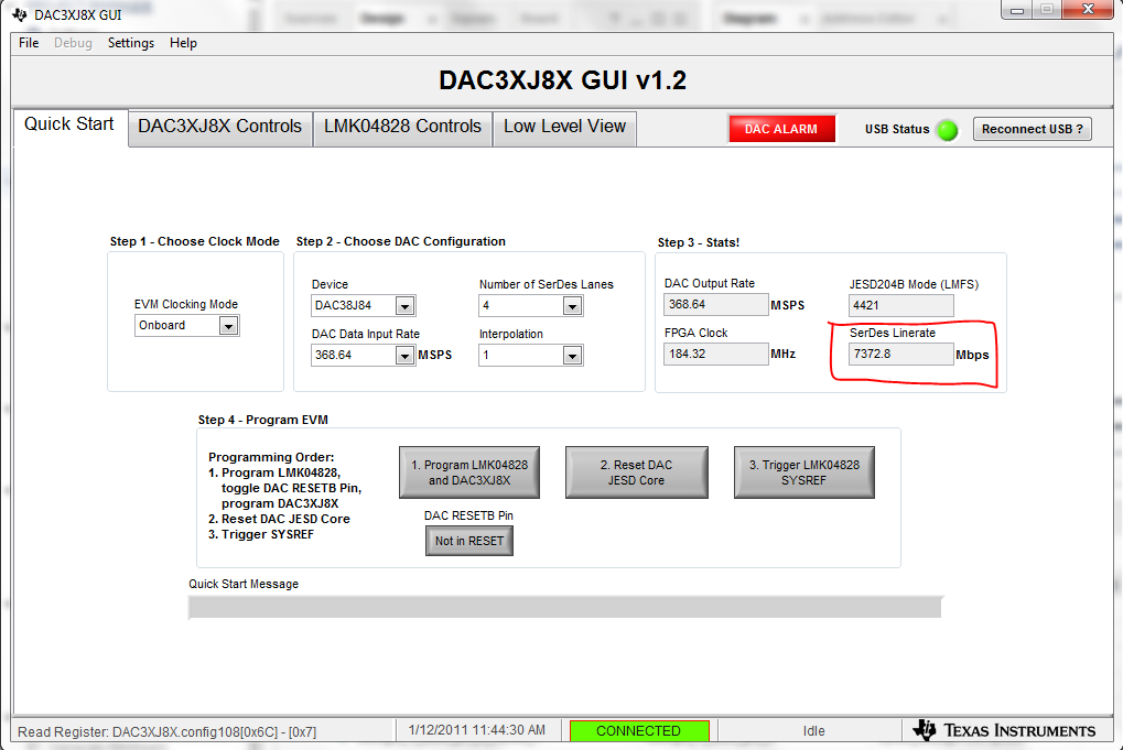
I'm using ZCU102 and DAC38J84EVM board. 

1. Program DAC38J84    (no alarm in DAC GUI)   (I'm using lane 0-3)

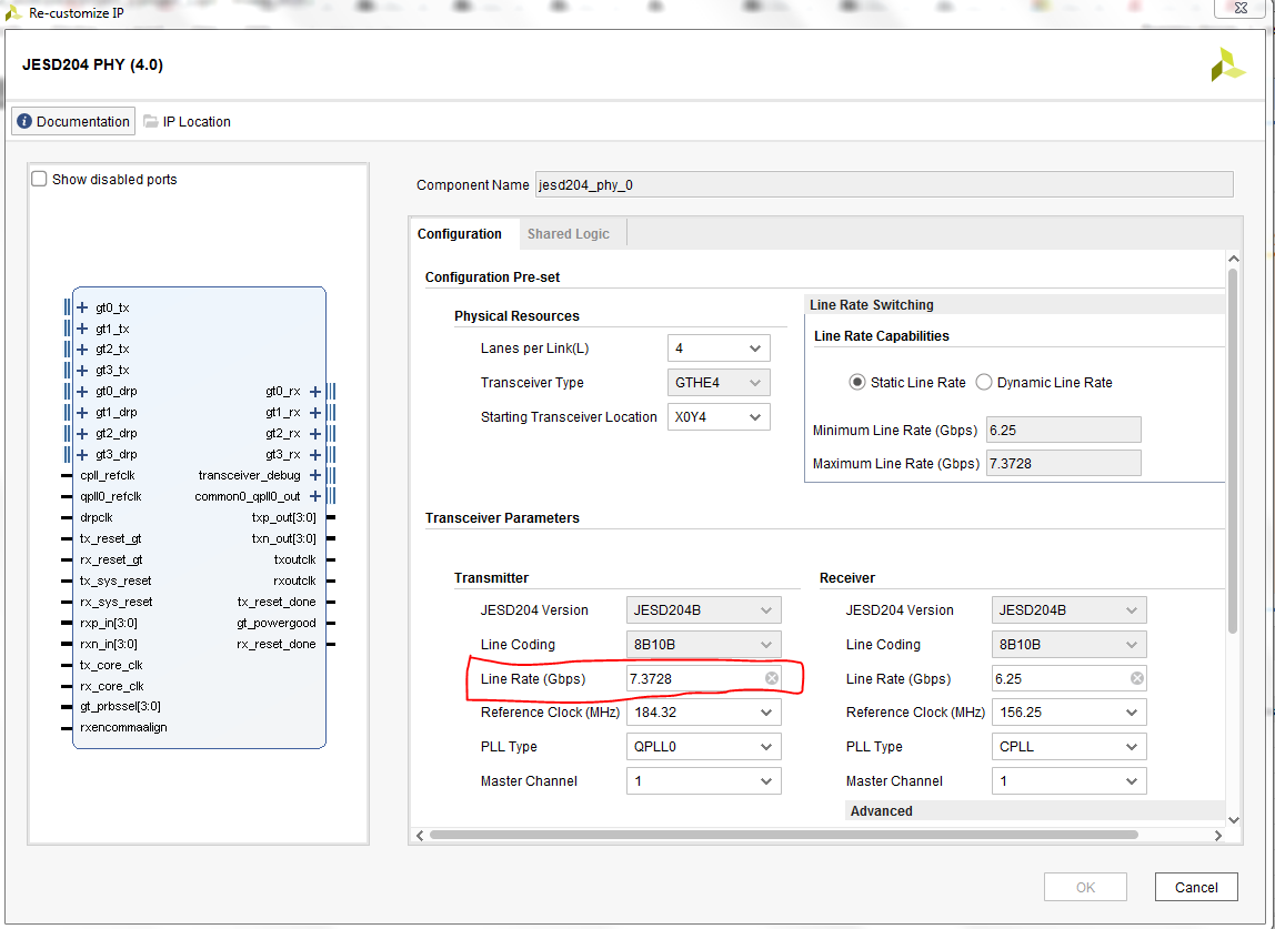
2. Program FPGA      (no alarm in DAC GUI)

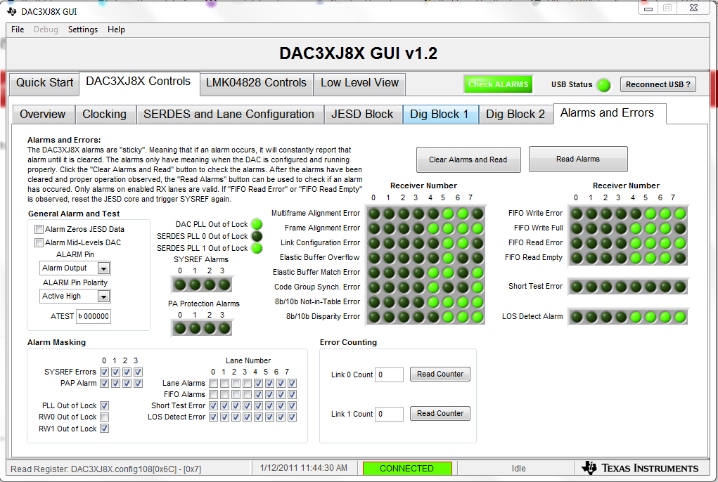
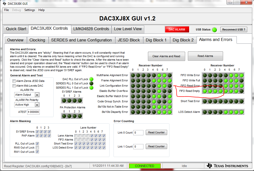
3. Reset DAC JESD Core    (FIFO read empty alarms shown on received lanes)

4. Trigger SYSREF      (no alarm, SYNC asserted, FPGA JESD Tx starts transmitting data, but no DAC output, always 670 mV current)

Questions:

a. I think it's weird, if the FIFO is empty means no K characters received at DAC, then how can it get SYNC asserted. Or is that normal to get FIFO empty alarm before CDS. 

b. If FIFO read empty happens, what might be the cause, and how to debug it

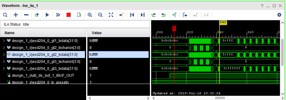
c. I can pass the NCO test alone(hardware level should be fine), but still can not get any output with the (see capture below) FPGA JESD Tx Core, seems it pass the CDS, LAS and starting transmitting. What might cause this?

Regards,

Yawen


  • Yawen,

    FIFO empty error indicates there is a SERDES rate mismatch between FPGA SERDES transmitter and DAC SERDES receiver. The DAC SERDES receiver (SRX) has a FIFO in between the SRX block and the JESD204B RX block of the DAC. The clock at the input of the FIFO is basically recovered clock from the DAC SRX with the source being the STX of the FPGA. If there are FIFO empty error, the STX of the FPGA is not matching up with the SRX rate of the DAC.

    Also, the JESD204B specification requires the JESD204B TX (on the FPGA side) need to be initialized before the JESD204B RX of the DAC. This is to prepare the JESD204B logic device to accept the ~SYNC handshaking signal from the JESD204B RX of the DAC. You may need to consider this step and figure out what is needed to change between your step 1 and 2. Keep in mind I am only referring to the state machine configuration, not necessary the entire logic design.

    -Kang

  • Hi Kang,

    Thanks for your time! I'm trying to changing my program sequence as you mentioned. As for the SERDES rate mismatch, I've set both FPGA Tx Core and DAC SerDes Linerate as 4.9152 Gbps. Is there other parameters I'm missing?  I'm providing 184.32MHz clock sourcing from LMK04828 for both FPGA core clock and the reference clock. Thanks for your time.


  • Yawen,

    One tip: you cannot just change the sequence from 1 to 2 and 2 to 1. There are many steps within these main steps that you need to break it down and analyze.

    The main thing is that the JESD204B TX fabric has to be up and running before DAC initialization and the JESD204B RX of the DAC. 

    Your lines rates are at 7.3728Gbps, however you mentioned 4.9152Gbps. There is a mismatch.

    Take a look at our example firmware. Search TSW14J10EVM on our website for example firmware design. We cannot help you on the FPGA design.

    -Kang

  • Thanks Kang, I'll look into it.