This thread has been locked.

If you have a related question, please click the "Ask a related question" button in the top right corner. The newly created question will be automatically linked to this question.

ADC12DJ5200RF: Random data in serial link

Part Number: ADC12DJ5200RF


I'm using the ADC12DJ5200RF-EVM Rev B in JMODE3 to interface with a Stratix 10 FPGA. The receive side of the JESD link uses Intel JESD204B IP, which has worked when I used the ADC12DJ3200-EVM. I've gotten the link up, with K = 20, but I see bad data mixed with expected samples.

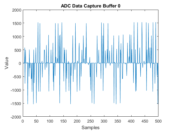
The images below show the data stream at the output of the Intel JESD204B Receiver IP, at the link clock rate, before (jesd_link_*_data) and after (tpl_data_*_out) the transport layer. These images were captured with no input stimulus, so I'd expect values near zero.

Signal Tap, pre and post transport layer:

Plotted, post-transport layer:

I'm thinking that maybe my external sample and reference clocks are bad, but both share a common 10 MHz reference and look mostly clean on a spectrum analyzer. My sample clock is 9 dBm and reference clock is 6 dBm. I'm not sure why this is happening, could it be the JESD204C protocol has extra alignment words periodically sent around the data?

Thanks,

Ryan

  • Ryan,

    We are looking into this.

    Regards,

    Jim

  • Thanks Jim.

    I captured more data using the transport layer test mode, and it appears that some lanes have persistent bit errors. It also appears that the lanes are not in the order I expected them to be based on my pinout.

    Link A
    Expected Observed Frame Data
    DA7      ?        47A 5F0 5A 7 856 5A4 D
    DA6      ?        E91 9FF A9 3 919 4BE F
    DA5      DA4      B41 B42 B4 3 B44 B45 0
    DA4      DA5      A51 A52 A5 3 A54 A44 0
    DA3      DA7      871 872 87 3 874 875 0
    DA2      DA6      961 962 96 3 964 965 0
    DA1      ?        0FA 202 F2 3 FE4 EDF 0
    DA0      DA1      E11 E12 E1 3 E14 E15 0


    Perhaps the physical lanes on the EVM are not routed to the pins shown in the schematic? I have DC061_ADC12DJ5200RF_EVM_SCH_RevB(001).pdf:


    I'm confused because the JESD receive side in the FPGA reports all good status, all lanes locked to data and I don't see anything wrong. Yet the data on some lanes is full of errors. The only thing left to try I think is to probe the FMC pins directly on the EVM board. 

  • Hi Ryan,

    Can you please make sure the scrambling is enabled on the receiver side? Because if you are using the ADC12DJ5200RFEVM GUI to program the ADC. The scrambling is enabled by default. Also can you use ramp test pattern and check if you are capturing the Ramp on FPGA. In ramp test pattern mode. The ramp is send on each lane and it counts from 0x00 to 0xFF.

    Regards,

    Neeraj