A related question is a question created from another question. When the related question is created, it will be automatically linked to the original question.
If you have a related question, please click the "Ask a related question" button in the top right corner. The newly created question will be automatically linked to this question.
please help to review the DS90UB960WRTDRQ1 schematic
- For the power supply decoupling, please make sure that you have allocated enough 0.1uF/0.01uF caps so that you can follow the datasheet guidelines for placing those caps close to each pin which requires local decoupling
- I can't really tell what is going on with the I2C connections. The I2C pins appear to be connected to many nets labeled as GPIO that go off page. Please make sure that these pins are only connected to an I2C controller off page and also do not connect the two buses to eachother
- There is a table which lists out the resistors for corresponding MODE strappings in the schematic but it doesn't appear to match the actual resistor values which are shown in the schematic. I recommend using the datasheet recommended resistors for all MODE strapping options
- Recommend populating C87 to ensure that the PDB doesn't float high during power up before the supplies are ramped and stable. If PDB is going to be pin controlled, then add an external pulldown instead of external pullup to ensure the rail is not pulled high before the GPIO is initialized
- Oscillator part number is not shown but please ensure oscillator meets REFCLK stability requirements and jitter requirements listed in the datasheet
- Tie pin 4 directly to GND only, no resistor and no strapping option for pulling it high. This pin is actually reserved (see datasheet)
- Not sure why GPIO6 and GPIO5 are connected to each other. Any reason for this?
For these comments in the schematic:
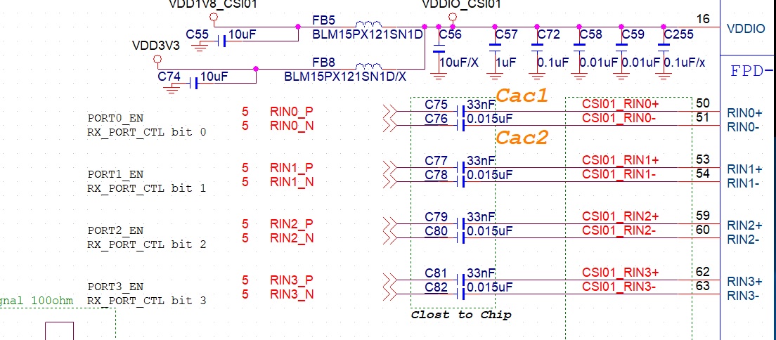
DS90UB913A-Q1 and DS90UB933-Q1 R1=4.02K R2=4.02K L2=10uH Cac1=100nF Cac2=47nF L1=100nF
- For the power supply decoupling, please make sure that you have allocated enough 0.1uF/0.01uF caps so that you can follow the datasheet guidelines for placing those caps close to each pin which requires local decoupling
=>OK
- I can't really tell what is going on with the I2C connections. The I2C pins appear to be connected to many nets labeled as GPIO that go off page. Please make sure that these pins are only connected to an I2C controller off page and also do not connect the two buses to eachother
=>Update i2c block diagram. (As attached)
Q: How do we control the initial flow when we use 2CH of CSI output on a single TI960?
Q: Is it possible that when we initialize the second CSI output, the CSI output will have a short delay?
Q: What is the purpose of the second group of I2C? Can I use I2C_SCL to complete all settings? (Including CSI0 / CSI1)
- There is a table which lists out the resistors for corresponding MODE strappings in the schematic but it doesn't appear to match the actual resistor values which are shown in the schematic. I recommend using the datasheet recommended resistors for all MODE strapping options
=>Remove the extra notes.
- Recommend populating C87 to ensure that the PDB doesn't float high during power up before the supplies are ramped and stable. If PDB is going to be pin controlled, then add an external pulldown instead of external pullup to ensure the rail is not pulled high before the GPIO is initialized
Q: How do we control the initial flow when we use 2CH of CSI output on a single TI960?
Select the desired CSI-2 ports with register 0x32, forward RX ports to the desired CSI-2 outputs with register 0x20
Q: Is it possible that when we initialize the second CSI output, the CSI output will have a short delay?
You can initialize them both at the same time if you select both CSI-2 ports for writing commands with register 0x32
Q: What is the purpose of the second group of I2C? Can I use I2C_SCL to complete all settings? (Including CSI0 / CSI1)
You can connect multiple SoCs to the 960 using multiple I2C ports. That way separate processors can both control the 960 and access the remote imagers if needed. Only one I2C port is needed to configure all settings. The second is optional.
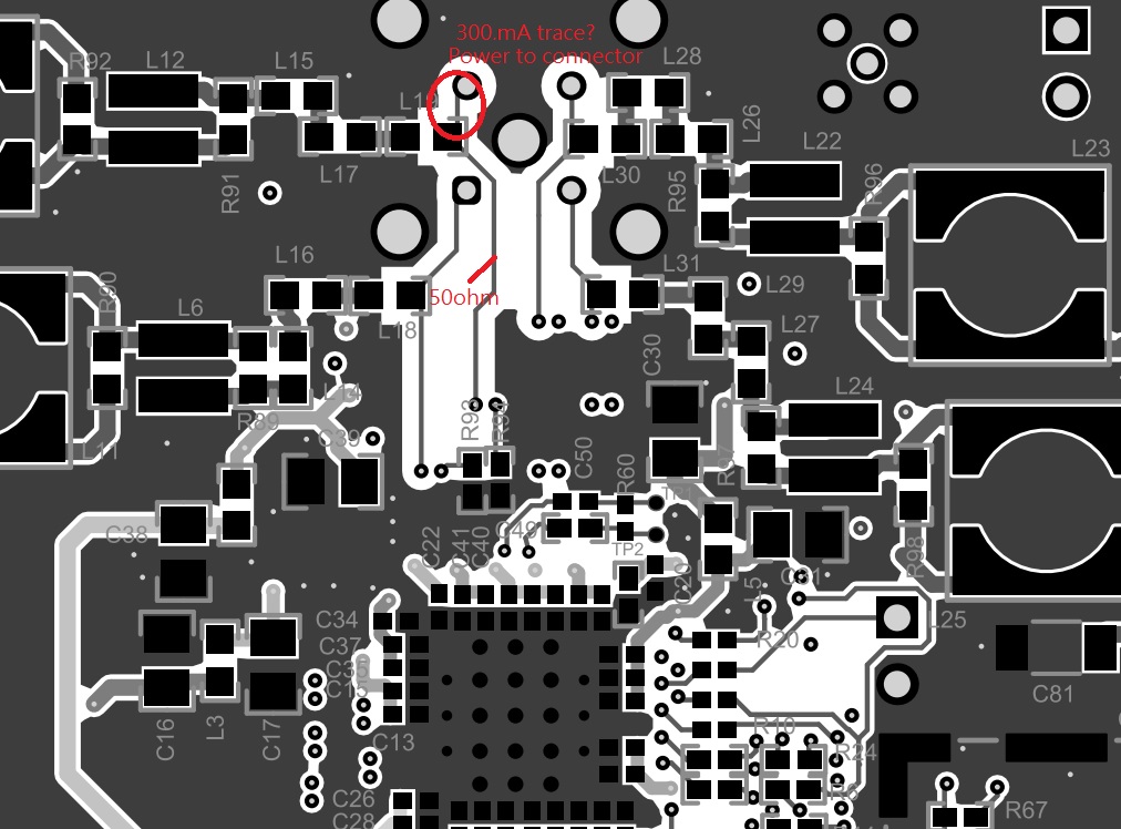
If I chip and connector of a long distance, Such cac1 & cac2 to close chip or connector? (It seems to be close to the chip)
In addition, I refer to the layout of the EVM. The PCB trace from Power to Connector is not widened. Can the current output 300mA~500mA? (How many mil? We 50ohm is 5mil, Is this enough?)
Can you provide EVM board file for us layout reference?
It is recommended to place the AC coupling caps as close as possible to the IC rather than the connector. The recommended PoC network from the datasheet is not suitable for 500mA current. It is only suitable for ~250mA max. If you need to supply more power, it is recommended to increase the PoC voltage.
I will send you a private E2E message with the EVM file for reference.
Yes 5mil should no issue for 250mA. The oscillator specification does not look good because the electrical parameters are only specified at room temp. See the notes on page 3.
I would suggest finding an oscillator which has electrical characteristics specified across the entire operating temp of the device.
For supporting ~30m cable it would be recommended to implement a repeater solution as you mentioned. ex. 953 -> 954 -> 953 -> 960
For PoC, it is highly recommended to increase the PoC voltage in order to deliver higher power with lower current. Can you increase the PoC voltage? What is the total required power delivery?
We do not currently have a single chip repeater solution.
For the PoC, 10W is very high. We do have some 1A solutions available from our passive vendor partners. If you would like then I can put you in contact with those vendors for qualified solutions.