This thread has been locked.

If you have a related question, please click the "Ask a related question" button in the top right corner. The newly created question will be automatically linked to this question.

TLC2558: TLC2558 I

Part Number: TLC2558

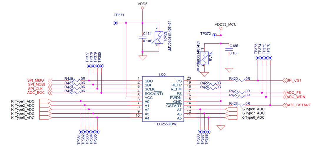
Hello, we have a project using Atmel ATSAM4E8E platform to drive TCL2558 ADC converter.

Now we can't use it even we follow the datasheet to set.

we are according to datasheet to building whole read process,

But we can’t successful read ADC value in below process.

Step as below:

1. Writing 0xA0C0 to setting mode is sweep mode.

2. written 0x9000 to read CFR register value

3. start convert by pull down CSTART

4. waiting for INT pin trig

5. written 0xE000 to read FIFO data

In step 2, we can;t to read CFR data successful after write 0x9000 command.


We tried to read single ADC value (one shot mode),

Step as below:

1. written 0xA000

2. written 0x9000 to read CFR register value

3. start convert by pull down CSTART

4. waiting for INT pin trig

5. read ADC value and write next ADC channel if you want read.

Same with sweep mode, the interrupt had no occurred, we don’t know what we are ignore some things in above steps.


We tried to read and write data when SCLK falling edge

But we have no read any value on SPI bus,

And we written data when SCLK rising edge, the SPI receiver had value, but it is different with write data.

So we are confusing in this timing diagrams, when did the SPI trig?


If we use "one shot" to read ADC, could we ignore to write CFR?

Thanks,

Best Regards,

Johnnie

  • Hi Johnnie,

    Welcome to our e2e forum!  Can you provide a schematic and a scope shot of your control signals?  Pulling /CSTART low only begins the sampling process, the TLC2558 won't start its conversion process until you bring /CSTART back high.  Assuming SCLK is running, the INT output should go low once the conversion process is complete.

  • Hi Tom,


    >>>The TLC2558 won't start its conversion process until you bring /CSTART back high. 

    Yes, we have pull /CSTART back high.


    >>Can you provide a schematic

    Please see as below

    >>>Can you provide a scope shot of your control signals?

    We follow below timing chart to set.

    Do you have the setting process or any suggestion?


    Best Regards

    Johnnie

  • Hi Johnnie!

    Thanks for the schematic - can you please send the actual control signals from your processor?  I know the timing diagrams in the datasheet, but I don't know how you are actually applying your signals.  This is important to help debug what might be going on at your end.

  • Hi Tom,

    >>can you please send the actual control signals from your processor?  

    Please see as below:

    We write 0xA000 Then we want to read CFR register so write  0x9000 to TLC

    But TLC2558 SDO data output not the same as datasheet. 

    Best Regards

    Johnnie

  • Thank you Johnnie,

    A couple of observations - first is that you are sending 0xA000 using the rising SCLK edge and then your 0x9000 uses the falling SCLK edge.  You are also not using the FS input, so you should be looking at the timing diagrams which say (FS=1, FS is not used).  When FS is not used the SDI should be valid on the rising SCLK edge.  Use Figure 16 as your guide to the timing requirements of your TLC2558 setup.  SDO in this mode should be valid on the rising SCLK, so you may need to zoom in a bit on your LA plot to see if that condition is true.

    So, send your 0xA000 and 0x9000 (and any other command) with valid data on the rising SCLK, and don't change the polarity of you clock as you did above for the second cycle.

  • Hi Tom,

    We follow your suggestion to set as below:

    >>SDO in this mode should be valid on the rising SCLK

    Step 1:

    We wriet 0xA000

    Step 2:

    We write 0x0600 to set CFR

    Step 3:

    Read CFR 0x0900

    Step 4:

    Read CFR 0x0900

    Is that correct?

    We also have another question.

    The TLC 2558 seems output SDO by falling edge SCLK.

    Is that correct?

    If right, our platform are using ATMEL SAM4X8X that SPI mode can't read falling edge of SCLK.

    Because we already set to rising SCLK mode.

    How can we  solve this situation?


    Thanks & Best Regards

    Johnnie

  • Hi Johnnie,

    Not quite there yet, you initialize the part with the 0xA000 and then write to the configuration register with 0xAxyz, where 'xyz' are the specific bits that you want to set.  I see what looks like a 9th SCLK in the very first transaction in the latest screen shot you sent.  Can you trigger on the /CS line and capture the first transaction?

  • Hi Tom,

    We write the CFR as below:

    The first transaction as below:

    The output seems like falling edge of SCLK.

    Do you know how to change this output mode to rising edge of SCLK?

    Thanks & Best Regards

    Johnnie 

  • Hi Johnnie,

    It looks like you are making some progress!  At least the INT is toggling now!  Before you try to get going with extended sampling, please let me know if the CFR readback is correct.  As I mentioned, Figure 16 is what you should be looking at and you do have a really slow (relatively speaking) SCLK.  Compare the setup/hold time provided by the TLC2558 to those required by your CPU.

  • Hi Tom,

    >>Figure 16 is what you should be looking at and you do have a really slow

    You are right.

    The Figure 16 is very important.

    Our SPI CLK setting frequency is too slow.

    After we adjust the SCLK Low 25ns -- Hi 25ns that we can read the ADC data.

    But now has other question...noise to effect the converter data.

    The converter data is not stable.

    Do you have any suggestion of this?

    Thanks & Best Regards

    Johnnie

  • Hi Johnnie,

    I'm happy to hear its working better for you!  Can you get screen shots using an oscilloscope rather than the logic analyzer?  Chip select, SDI, SDO and SCLK should be good enough.

  • Hi Tom,

    >>Can you get screen shots using an oscilloscope rather than the logic analyzer? 

    You can see as below:

    The SCLK can't be Hi & Lo.

    We try to pull 4.7K ohm (with SCLK ,MISO, MOSI)  to Vcc..

    It also has no effect.

    The CS is noise effect scope channel 1.

    We also check ATMEL4X8X SPI spec.

    Thanks & Best Regards

    Johnnie

  • Looks like grounding and clock termination issues.  How fast is your SCLK now?  If the scale is right, it looks to be ~30MHz.  Can you slow it down to maybe 10MHz and see what it looks like?

  • Hi Tom,

    >>How fast is your SCLK now?  

    We set the SCLK frequency for 20 MHz.

    >>Can you slow it down to maybe 10MHz and see what it looks like?

    We set the SCLK to 10MHZ.

    Please see as below:

    Thanks & Best Regards

    Johnnie

  • Hi Johnnie,

    These captures look much cleaner!  The SDO seems to transition a little low, but that may be related to some capacitive loading on your PCB.  Since the CFR read back issue seems to be cleared up, I'll close out this thread and let you work a little more closely with Ben.

  • Hi Tom,

    Thanks for your help.

    But even we slow down the SCLK frequency let these signal clean.

    We read the transfer ADC data that the data should shift right 1 bit.

    And if we follow the Figure 16 timing to set.

    That the output ADC data is not correct.

    We use K-Type to detect temperature and read the ADC data from TLC2558.

    The transfer data is very  strange.

    Finally thank you for solving most problems.

    Best Regards

    Johnnie

  • Hi Johnnie,

    Has Ben gotten in touch with you yet?  If you are connecting the K-Type thermocouples directly to the inputs of the TLC2558, that might be part of the problem.  You may need to buffer the inputs first and I would also like to see an R/C filter ahead of each channel.  Perhaps you have that already on another page of your schematic.  We have a series of training videos on driving a SAR ADC that you might find useful as well.

  • Hi Tom,

    >>Has Ben gotten in touch with you yet?  

    Yes, he had.

    >>You may need to buffer the inputs first and I would also like to see an R/C filter ahead of each channel.

    Please check as below:

    J28 connector is connect to K-Type.

    Is possible the R435 & C195 issue?

    The R range 10 - 100 ohm & C is 50 pf,  is it right?

    other question

    Our Vcc is 5V.

    Is this TLC2558 only use at SCLK 20 Mhz?

    Why the Pulse width TwL & TwH min is 20 ns?

    That mean we can set the SCLK to 25 Mhz, is it right?

    We confuse it.


    Thanks & Best Regards

    Johnnie

  • Hi Johnnie,

    The pictures/files you sent did not come through.  The SCLK is MAX 20MHz, the twL and twH times represent the worst case duty cycle of the SCLK - 20/30 low/hi or 30/20 low/hi.

  • Hi Tom,

    >>The pictures/files you sent did not come through.  

    J28 connector is connect to K-Type.

    Is possible the R435 & C195 issue?

    The R range 10 - 100 ohm & C is 50 pf,  is it right?

    Thanks, & Best Regards

    Johnnie

  • Hi Johnnie,

    Those values are quite high actually considering the input to the ADC.  Try reducing R435 to maybe 100 ohms and C195 to 47pF and see if that improves things for you.

  • Hi Tom,

    The original schematic R435= 100 Kohm & C195= 1uF 

    And then we setting SCLK 20 Mhz 

    We capture the result as below :

    We find that the temperature stop at 25.7 degree

    But it should be 30.7 degree.

    After we set the  R435= 100 ohm & C195= 47pF 

    And then we setting SCLK 20 Mhz

    The Temperature detect become worse.

    You can see as below:

    In case we slow down SCLK frequency and then the result  shift 1 bit.

    We can get the temperature as below

    Thanks & Best Regards

    Johnnie

  • Hi Johnnie,

    I'm not sure why you would stop at 25.7 with the original configuration, and I don't understand exactly how you are converting your hex values to temperature, but something does not seem right.  The TLC2558 is a 12-bit device and if you are running with 16 clock transfers, you should have a max value of 0x0FFF.  I would expect to see the LSB's toggle some what and your display shows the last nibble always as '0'.  Are you left shifting your data before you put it out on the COM port?

  • Hi Tom,

    >>you should have a max value of 0x0FFF.

    Yes, we can get the 12 bit value by read internal test channel.

    1011b B000h Select test, voltage = (REFP+REFM)/2
    1100b C000h Select test, voltage = REFM
    1101b D000h Select test, voltage = REFP

    >>Are you left shifting your data before you put it out on the COM port?

    Yes, after we get the B0 & B1 we shift 4 bits to calculate the temperature.

    You can see below program.

    e_SPI_writeAndRead(SPI_CHIP_DAC, u32_csPin, txData, rxData, 2);==>SPI read ADC data


    dataBuf[0] = ((rxData[0] << 4) | (rxData[1] >> 4)); ==> we shift 4 bits
    printf("ADC_R B0 = %x, B1 = %x\r\n",rxData[0],rxData[1]); ==> print out to com port.

    f32p_rxData[0] = (float)((dataBuf[0] * 0.000805) / 0.005); ==> transfer the value to temperature

    printf("Tmp%d = %d\r\n", i, (uint16_t)(f32p_rxData[0]*10)); ==>print out to com port.

    So the B0 = 0x09 & B1 = 0xC0 that after sfift 4 bits we can get dataBuf[0] = 0x9C = 156.

    The Tmp = 156 * 0.000805/0.005 = 25.1 degree

    So you can see 251 value on com port.

    Thanks & Best Regards

    Johnnie