This thread has been locked.

If you have a related question, please click the "Ask a related question" button in the top right corner. The newly created question will be automatically linked to this question.

ADS124S08EVM: ADS124S08: time to get data after changing the input channel

Part Number: ADS124S08EVM
Other Parts Discussed in Thread: ADS124S08, REF5025,

Hi there,

I've some troubles with the measuring of three input channels where a 3-axis force sensor is connected. My general question is, how long it takes to get valid data when the input channels (differential mode) are changed or switched to another inputs? With a logic analyser by inspecting the /DRDY pin it takes independent of different configurations around 57 ms (milliseconds) but to get a good measurement with the force sensor I want the get all three channels within below 3 ms. The background is that we have to measure hundred times a second the sensor, thus each 10 ms all three channels has to be measured.

My general question is, is there any chance to do it with the ADS124S0x? In very short I only use differential inputs (A0/A1, A2/A4, A8/A9), the external on-board reference (2.5V), the internal clock, and the low latency filter. The gain is set to 128.

If you need more information about this like hardware setup or configuration and read-out procedure, please let me know. Currently I can read out the values from the three channels and calculate the voltage from this and these results meets the voltage at the inputs.

  • Hi Klaus,

    Are you trying to get the 3-axis result using the EVM and EVM GUI?  If so, using the scripting portion of the GUI will be too slow as there are a number of required internal delays required to keep the communication in sync. To actually use the EVM, a separate controller and different set of firmware would be required.  There is example code on the web at:

    http://www.ti.com/lit/zip/SBAC159?jktype=tools_software

    The ADS124S08 is in itself capable of reading all of the axis within 3ms, but will require that you use 2ksps as a minimum.  See Table 13 of the ADS124S08 datasheet for the conversion times for the low-latency filter.  You will need to use the timing from the First Data column and also add the internal delay from the programmable delay setting in the Gain setting register.  The default value is 14*tmod periods.

    When reading one conversion result you can set up the configuration for the next one at the same time by following the information in section 9.5.4.3 on page 71 of the ADS124S08 datasheet following the timing in Figure 92.

    Best regards,

    Bob B

  • Hi Bob,

    the whole morning I was now busy to reply and nearly finished with my answer and then the browser crashed by uploading a screenshot. As you can imagine this is very very annoying. To this issue I wrote a suggestion in the site support forum. However, I will describe my issue in more detail.

    Bob Benjamin said:

    Are you trying to get the 3-axis result using the EVM and EVM GUI?

    At the beginning when I took the first steps with the EVM I was using it but I was very disappointed about it. After each commando I sent to the EVM the EVM did not response so I've to reset the EVM after each commando. Later, when I begun to develop our firmware, I found out that the ADS124S08 didn't response to any commando I sent directly via the SPI connection. After some examination with the logic analyser (LA) and later with an oscilloscope I found out that the bus coupler U3 (TXS0108ERGYR) was swinging around 40 MHz sinusoidal on nearly each pin.So I've removed this chip and after I took a closer look to the schematic and my development environment I found out that i don't need that because the processor and the ADC are running with the same voltage (3.3 V). After removing the bus coupler U3 I've direcly connected the five necessary lines directly, thus A4 with B4 (ADC_DRDY), A5 with B5 and so on until A8-B8. The rest is still open thus A1/B1 to A3/B3. Additionally I've added three pull-up resistors (3k3 each) to the /CS and SCLK, the /RESET pin is also connected via a 3k3 resistor to Vdd (3.3 V). Over the J3 connector the EVM is connected to the microcontroller of the other development board. I hope that's so far OK and that the connected TIVA have no effect to the rest. By the way, the EVM is feeded also via the J3 connector with 3.3 V. I' make no use of the USB connector.

    Bob Benjamin said:

    To actually use the EVM, a separate controller and different set of firmware would be required.

    That is exactly that what I'm doing now and it works as expected so far.

    Bob Benjamin said:

    The ADS124S08 is in itself capable of reading all of the axis within 3ms, but will require that you use 2ksps as a minimum.  See Table 13 of the ADS124S08 datasheet for the conversion times for the low-latency filter.  You will need to use the timing from the First Data column and also add the internal delay from the programmable delay setting in the Gain setting register.  The default value is 14*tmod periods.

    I have checked out this configuration and here are my results. I've made few screenshots, I hope this will be helpful and make several things more clearly. The describing text is below each screenshot.

    Here you can see the initialisation of the ADC. The LA is triggered on the falling edge of /CS. At first, I've to reset the ADC..

    After a while the initialisation of the ADC begins. At the end I read back the whole configuration registers. The values of this registers are as follows. I've coloured the registers which are not at default value.

    MOSI 0x20 0x12 0x00 0x00 0x00 0x00 0x00 0x00 0x00 0x00 0x00 0x00 0x00 0x00 0x00 0x00 0x00 0x00 0x00 0x09
    MISO 0x00 0x00 0x08 0x00 0x01 0xEF 0x14 0x10 0x00 0xFF 0x00 0x50 0x00 0x00 0x00 0x00 0x00 0x40 0x00 0x00

    The non-default value registers and it's deviations:

    Device Status Register (address 0x01) = 0x00, seems to be OK, POR has been cleared

    Gain Setting Register (0x03) = 0xEF, delay = 0b111 = 1 * t_MOD (this seems to be not resetted after a reset commando, other register shows the same effect), PGA enabled, gain set to 128

    System Control Register (0x09) = 0x50, system monitor = internal temperature sensor measurement enabled

    The ADC is in continuous conversion mode and here is the problem I have. It takes 50 to 60 ms that the DRDY pin goes low. I do nothing with the DRDY pin inside the software, this pin is also not connected to any hardware except to the an input pin of the logic analyser. In the source code I've added a delay of 57 ms. After this time the DRDY-pin is in low-state and I can read the ADC value back. When beginning to read, the DRDY goes immediately high as described in the data sheet.

    This is a closer look to the read procedure. The read-out is started with 0x13 and then I get 3 bytes from the ADC. Unfortunately I get since yesterday wrong values back (0x7FFFFF) and I don't know why this is the case. Before this I got the right values back, for the channel-pair AIN0 (+) and AIN1 (-) it was 0x8DCACE (equals to something around 17..18 mV at the input pins), for channel AIN2/AIN4 it was 0xFFF980 (= -0.000... mV, this input is shorted and connected to GND so this value is ok), and for AIN8/AIN9 it was 0x0C540D (+/-1.883 mV).

    The last sequence is to switch over to the next channel, in this case to AIN2(+) and AIN4(-).

    Finally here you can see the whole measure sequence including the initialisation at the beginning (takes place only after reset the microcontroller) with the time and that is the problem until DRDY goes down. So a three-channel measurement cycle will take around 170 milliseconds and that is far to long.

    Can you see or have you any ideas what's could be wrong that it takes so much time?

    Bob Benjamin said:

    When reading one conversion result you can set up the configuration for the next one at the same time by following the information in section 9.5.4.3 on page 71 of the ADS124S08 datasheet following the timing in Figure 92.

    Yes, I've seen it but this is for later because the time I can save with this are only few microseconds if I'm right.

    Many thanks in advance!

  • To my regrets of the things happend and the time you spent on it, I found the mistake I've made. You're right, the datarate was not properly setted up. I forgot a line in the source code which writes the new datarate to the register.

    As you can see below, the DRDY-pin is now very active. A closer look to it shows me that the DRDY pin goes now down each 0,244 ms which is a sampling rate of 4000 SPS.

    Many thanks!

    Yours,

    Klaus

    PS: Do you know what could be the reason why I get only 0x7FFFFF as ADC value back from all three channels? I've measured all three inputs and the voltage did not change (A0/A1 = 1.879 mV, A2/A4 = 0.000 mV, A8/A9 = -18.371 mV).

  • Hi Klaus,

    I'm glad to hear you made some progress.  In your configuration for the reference you are using the default reference input of REF0.  I would double check that the external reference connected to REF0 is valid.  You could also try the internal reference to see if there is any change.  If the reference voltage is invalid or missing, it is quite possible to see full-scale readings.

    If the above is not the issue then you could look at something else.  I'm not sure how you are powering the sensor and the relationship of the output relative to the PGA common-mode, but you could verify that the inputs relative to AGND of the ADS124S08 are within the correct input range.  If the grounds are not connected between the sensor and the ADC you need to make sure that the output of the sensor is not attempting to drive the PGA to the supply rails.  I have seen a number of times where different AC to DC power supplies can have a much different output voltage relative to each other requiring a common ground point between them.

    Best regards,

    Bob B

  • Hi Bob,

    Bob Benjamin said:
    In your configuration for the reference you are using the default reference input of REF0.  I would double check that the external reference connected to REF0 is valid.

    A short update about this: Indeed, the reference voltage was not available due to a ugly connection on the EVM. Now this is fixed but the behaviour of the ADC is strange. Could it be that the ADC gets damaged if the external reference is not available? If I read out the ADC I always get independent from the selected input channel nearly the same value. There's only a difference in the last 6 or 8 bits. This value (calculated as  0.127.... V) did not change when the gain is set to 1, 2, 4, 8, 16, or 32. If the gain is set to 64, thus when I get a a by 2 digitally multiplied value, the the value is twice as high as the other gain factors. With a gain of 128 the value once again increases by the factor of 2, thus the calculated voltage at all inputs is slightly above 0.5 volt. I suppose that the ADC input is somewhere damaged but I didn't know what could be the reason for it.

    Bob Benjamin said:
    You could also try the internal reference to see if there is any change.  If the reference voltage is invalid or missing, it is quite possible to see full-scale readings.

    Thanks for your hint. I'm not very experienced with ADC's but this sounds logical to me. With this change I will check on Monday If I can read out different values from different inputs with different gain factors.

    For now I've already ordered a new EVM.

    Bob Benjamin said:
    I'm not sure how you are powering the sensor and the relationship of the output relative to the PGA common-mode, but you could verify that the inputs relative to AGND of the ADS124S08 are within the correct input range.

    This is a simple story. The force sensor consist of three strain gauges. The "upper" resistor has 375 ohm, the "lower" one 350 ohm. All together, the sensor needs 2.5 V / ((375 + 350) ohm / 6) = 20.7 mA. The onboard reference voltage can't drive the sensor, so I want to replace this reference with a stronger one which an output current of at least 30 mA. With this voltage, which is available at connector J9 pin 4 (not sure) and the GND, which is also available on J9 and J8 (depends on the jumper settings) I want to connect the sensor. For our prototyping issue this should be ok so far. Later, when the firmware part for the charge gauge is implemented, the whole design should run with a 3.7 V / 2000mAh battery which is connected to a buck-/boost converter (BQ27441) to get the 3.3 V for at least 8 hours.

    Bob Benjamin said:
     If the grounds are not connected between the sensor and the ADC you need to make sure that the output of the sensor is not attempting to drive the PGA to the supply rails.  I have seen a number of times where different AC to DC power supplies can have a much different output voltage relative to each other requiring a common ground point between them.

    You're right, a ground offset voltage can make big issues. But I don't believe that we create such an issue because only the sensor with it's 12 wires in total (4 wires each strain gauge) will be connected at J7, J8, and J9. The supply an digital interface will be connected at J3.

    Next Monday, when I'm back at work I will check the behaviour of the ADC when the configuration is changed to the internal reference. I will keep you informed.

    Thnaks so far,

    Klaus

  • Hi Klaus,

    If your sensor requires 30mA, then neither the internal reference or the external REF5025 has enough drive capability to directly excite the sensor.  I would try connecting an external voltage source to excite the sensor while also connecting the excitation source to REF0 inputs at J8 pin 1 (+) and J8 pin 4 (-).  You should also remove the jumper at JP8 to remove any source contention and JP11 should connect to the AGND position. This will allow the excitation source to also be the reference making the measurement ratiometric.

    As mentioned earlier, you could try the internal reference for the conversion measurement while using an external source for the excitation supply.  This should also work, but noise will be higher and drift could also be an issue long term.  A ratiometric measurement removes those issues.

    Best regards,

    Bob B

  • Hi Bob,

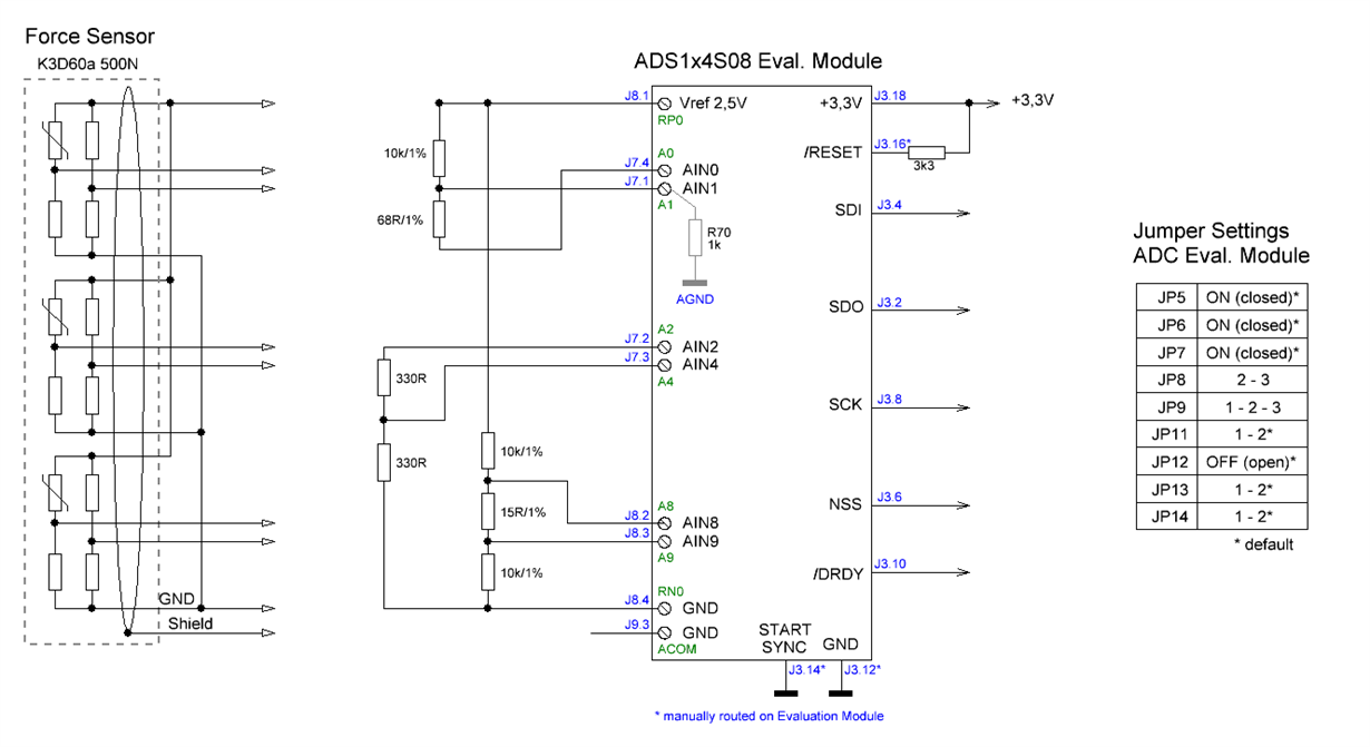
    To clarify the sensor supply, I want to replace the REF5025 (max. 10 mA output current) by a ADR431B, which is slightly stronger ( I_out max. 30 mA, 21 mA needed). The jumper on the EVM are set right (JP8 2-3 closed, JP11 1-2 closed). I hope this will not be an issue.

    The HW configuration is shown below. The resistors is the current setup what I'm using now, the sensor on the left what it should be.

    The voltage at the inputs are:

    AIN0 - AIN1: 18.378 mV, AIN2 - AIN4: 0.00 mV, AIN8 - AIN9: 1.887 mV, U_ref = 2.4994 V

    Now I've reconfigured the reference selection (reference control register), I switched over to the internal reference but without success. I suppose the the ADS124S08 is damaged but I've absolutely no clue what could be the reason for that. At all input channels, independed if they are shorted or not, I measure with a gain set to 1 at AIN0/AIN1 0.126963 volt, AIN2/AIN4 0.126992 volt, and at AIN8-AIN9 0.127031 volt. This value differs slightly if I measure these inputs again with a gain set to 2, 4, 8, 16, and 32. The values will increase by the factor of 2 if the gain is set to 64 and once again if the gain is set to 128.

    I had only one short moment last week where the values are that what I would expected. Then I had the upper-limit values (0x7FFFFF) and since I've fixed the ugly connection at JP9 the values are confusing me. So it's currently absolute not clear to me what the reason is for that. I've not changed anything at the EVM except that I've routed two tiny wires to GND as shown in the schematic above (SYNC/START and GND to a free J3-pin).

  • Hi Klaus,

    Just so I'm clear, your replaced the REF5025 with the ADR431 on the ADS124S08EVM, is that correct?  Have you verified that the reference output is stable (no oscillations)?  You may need to remove the capacitor connected to the trim pin for the ADR431. 

    Your diagram is not quite correct.  J7-1 does connect to AIN1, but does not connect to R70.  J7-4 does connect to AIN0 and R70.  If you measure across the 68 Ohm resistor using the configuration settings described earlier, you are using gain of 128 and PGA enabled, you will be outside of the input range of the PGA as described on page 8 in section 7.3 of the ADS124S08 datasheet.  The same is true for the 0V input at AIN2/AIN4 with the PGA enabled.  You should also verify that your connections are correct relative to J3 for GND, START/SYNC and RESET.  I realize that you are most likely using these not connected pins on J3 to make signal connections easier, but it is not really clear how these pins are actually connected.  Maybe a picture of your setup would help me verify.

    When looking at the conversion result, each time you change gain you should see the code value increase by a factor of 2 as each gain setting is increased.  In turn the full-scale range of the input is also decreasing by a factor of two. So the output code relates to the full-scale range.

    Let's target on the input voltage at AIN8/AIN9.  This input should be within the proper input range.  Can you give me a series of continuous and contiguous conversion results of about 256 to 512 results?  This will help me understand what is going on and whether noise is a factor in the results.  The other 2 sets of inputs will not be good data as they will be outside of the input range for PGA enabled at 128. Also, please give me the raw ADC result (preferably has hex values) and not converted to volts.

    Best regards,

    Bob B

  • Bob Benjamin said:

    Just so I'm clear, your replaced the REF5025 with the ADR431 on the ADS124S08EVM, is that correct?

    Not now, this I will be make later. For now everything is in the state as purchased on the ADC part (TIVA part is changed by removing U3). The external resistors which are now connectet to J7/J8 are only for simulation.

    Bob Benjamin said:

    Have you verified that the reference output is stable (no oscillations)?  You may need to remove the capacitor connected to the trim pin for the ADR431.

    Good news! I fixed the problem and the EVM IS NOT DAMAGED.

    The reason for the confusing measurements was a bug in the source code. During the configuration and setup procedure. The system control register (addr. 0x09) was configured that DVDD/4 measurement was set. With this the gain is set to 1. Another issue was the activating of the temperature sensor which was after reading not deactivated.

    Bob Benjamin said:

    Your diagram is not quite correct.  J7-1 does connect to AIN1, but does not connect to R70.

    Yes, you're right, my mistake when drawing this. R70 is connected to AIN0 so I can measure the same value at AIN0/AIN1, AIN2/AIN4, and AIN8/AIN9 with the ADC as with a multimeter.

    v[0] = -17.424165271222591
    v[1] = 0.0094994902610778809
    v[2] = 1.8857140094041824

    (values in mV)

    Bob Benjamin said:
    Let's target on the input voltage at AIN8/AIN9.  This input should be within the proper input range.  Can you give me a series of continuous and contiguous conversion results of about 256 to 512 results?  This will help me understand what is going on and whether noise is a factor in the results.  The other 2 sets of inputs will not be good data as they will be outside of the input range for PGA enabled at 128. Also, please give me the raw ADC result (preferably has hex values) and not converted to volts.

    Are you still interested? The I can modify the source code to do that. For now everything is done regarding the ADC.

    So far, thanks for your time helping me.

    Regards,

    Klaus

  • Hi Klaus,

    I'm glad to hear you found the issue.  I will consider this case closed.  If you have any further questions, please feel free to enter a new post.

    Best regards,

    Bob B