Other Parts Discussed in Thread: TMS320F2812,
Hi,
In a weigh scale project, I've encountered a strange problem. I've employed ADS1232, TMS320F2812 and SPI serial interface.
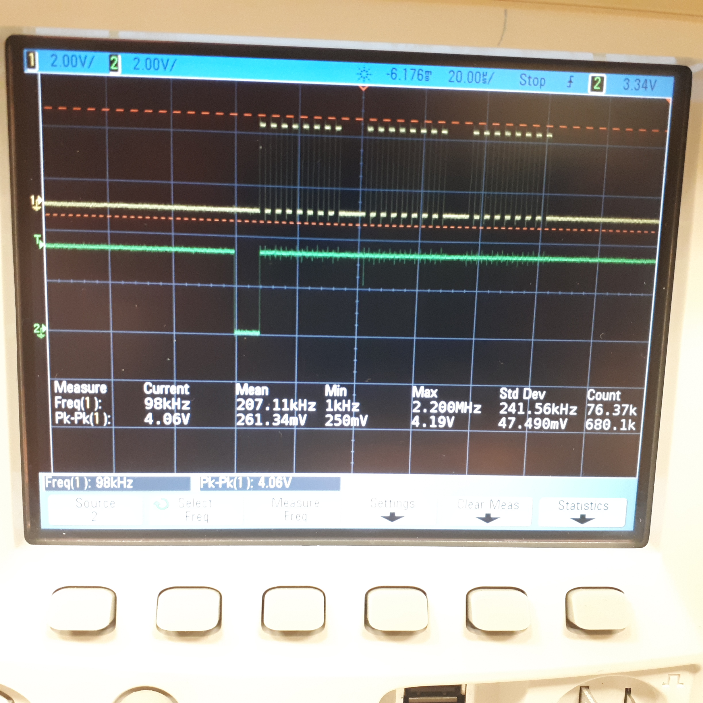
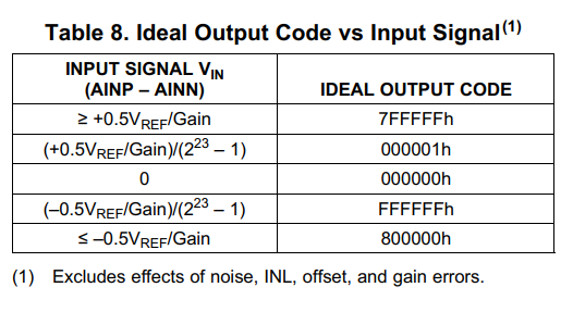
After each falling edge of DRDY, the data register is read, but it always is FFFFFF, independently of the input range,
sometimes 7FFFFF or 3FFFFF
use Weigh Scale Application schematic
my code:
use Spi Example:
include "DSP281x_Device.h"     // DSP281x Headerfile Include File
#include "DSP281x_Examples.h"   // DSP281x Examples Include File

// Prototype statements for functions found within this file.
// interrupt void ISRTimer2(void);
void delay_loop(void);
void spi_xmit(Uint16 a);
void spi_fifo_init(void);
void spi_init(void);
void error(void);
Uint16  Temp;
Uint16 sdata;  // send data
Uint16 rdata[3];  // received data


void main(void)
{
    Uint16 i=0;

   InitSysCtrl();
   InitGpio();  // Skipped for this example


   DINT;

  InitPieCtrl();

  IER = 0x0000;
   IFR = 0x0000;

  InitPieVectTable();

   spi_fifo_init();	  // Initialize the Spi FIFO
   spi_init();		  // init SPI
   InitXIntrupt();                 //Initialize external interrupt


       IER |= M_INT1 | M_INT6
       EINT;                           // Enable INTM
       ERTM;                           // Enable DBGM

       GpioDataRegs.GPBDAT.bit.GPIOB0 = 1;//enable ADS1232

       GpioDataRegs.GPFDAT.all = 0x0000;
       Temp=0xF0;


  for(i=0;i<3;i++) rdata[i]=0;
   sdata = 0x0000;
   for(;;)
   {
   }
}


void spi_init()
{                                                //0000 0000 0000 01111
	SpiaRegs.SPICCR.all =0x0007;	             // Reset.7(enable),POLARITY=0, SPILBK =0 , rising edge, 8-bit char bits
	SpiaRegs.SPICTL.all =0x0006;    		     // OVERRUN int.4=0 PHASE.3=0 ,Enable master=1, normal phase,
	                                             // enable talk.1=1, and SPI int.0 disabled.
	SpiaRegs.SPIBRR =0x007F;
    SpiaRegs.SPICCR.all =0x0087;		         // Relinquish SPI from Reset
    SpiaRegs.SPIPRI.bit.FREE = 1;                // Set so breakpoints don't disturb xmission
}

void spi_xmit(Uint16 a)
{
    SpiaRegs.SPITXBUF=a;
}

void spi_fifo_init()
{
    // Initialize SPI FIFO registers  //1110 0000 0100 0000
    SpiaRegs.SPIFFTX.all=0xE040;//SPIRST.15,SPIFFENA.14,TXFIFOrest.13 renable,
                                //TXFFST.12-8 ,TXFFINT.7, TXFFINT CLR.6, TXFFIENA.5,TXFFIL4-0
    SpiaRegs.SPIFFRX.all=0x204f;//RXFFOVF.15, RXFFOVF CLR.14, RXFIFOReset (Renable), RXFFST12-8
                                //RXFFINT, RXFFINT CLR, RXFFIENA.5, RXFFIL4-0

    SpiaRegs.SPIFFCT.all=0x0;   // FIFO transmit delay bits
}
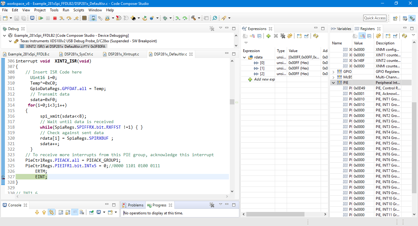
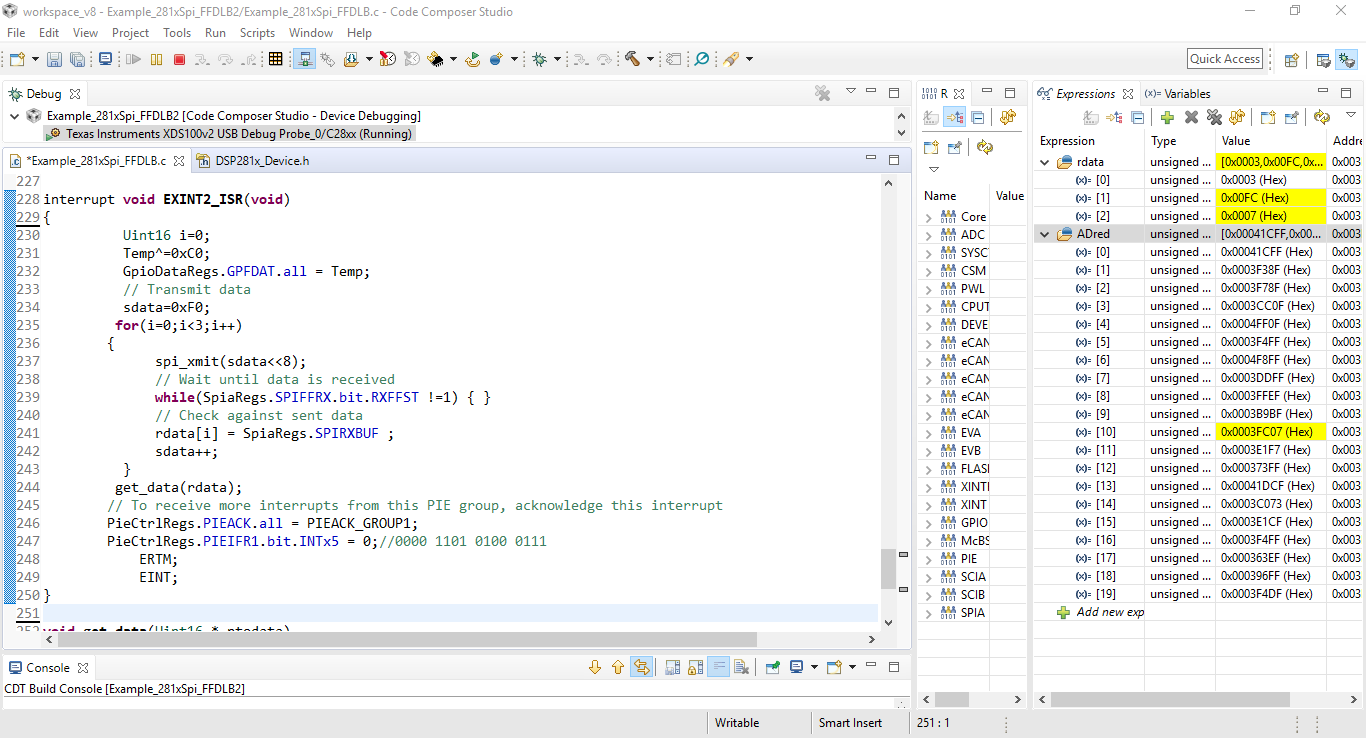
and XINT:
interrupt void  XINT2_ISR(void)
{
    // Insert ISR Code here
      Uint16 i=0;
      Temp^=0xC0;
      GpioDataRegs.GPFDAT.all = Temp;
      // Transmit data
      sdata=0xF0;
     for(i=0;i<3;i++)
    {
          spi_xmit(sdata<<8);
          // Wait until data is received
          while(SpiaRegs.SPIFFRX.bit.RXFFST !=1) { }
          // Check against sent data
          rdata[i] = SpiaRegs.SPIRXBUF ;
          sdata++;
      }