This thread has been locked.

If you have a related question, please click the "Ask a related question" button in the top right corner. The newly created question will be automatically linked to this question.

ADS1262: writing commande , DRDY

Part Number: ADS1262


hello ,

im using the ADS126xEVM REV A 

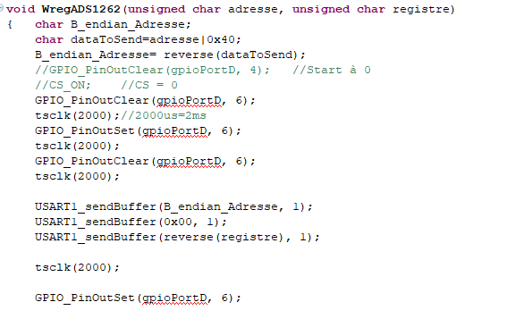
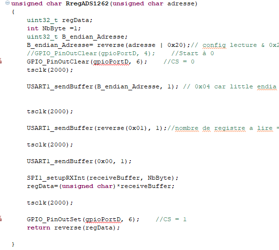
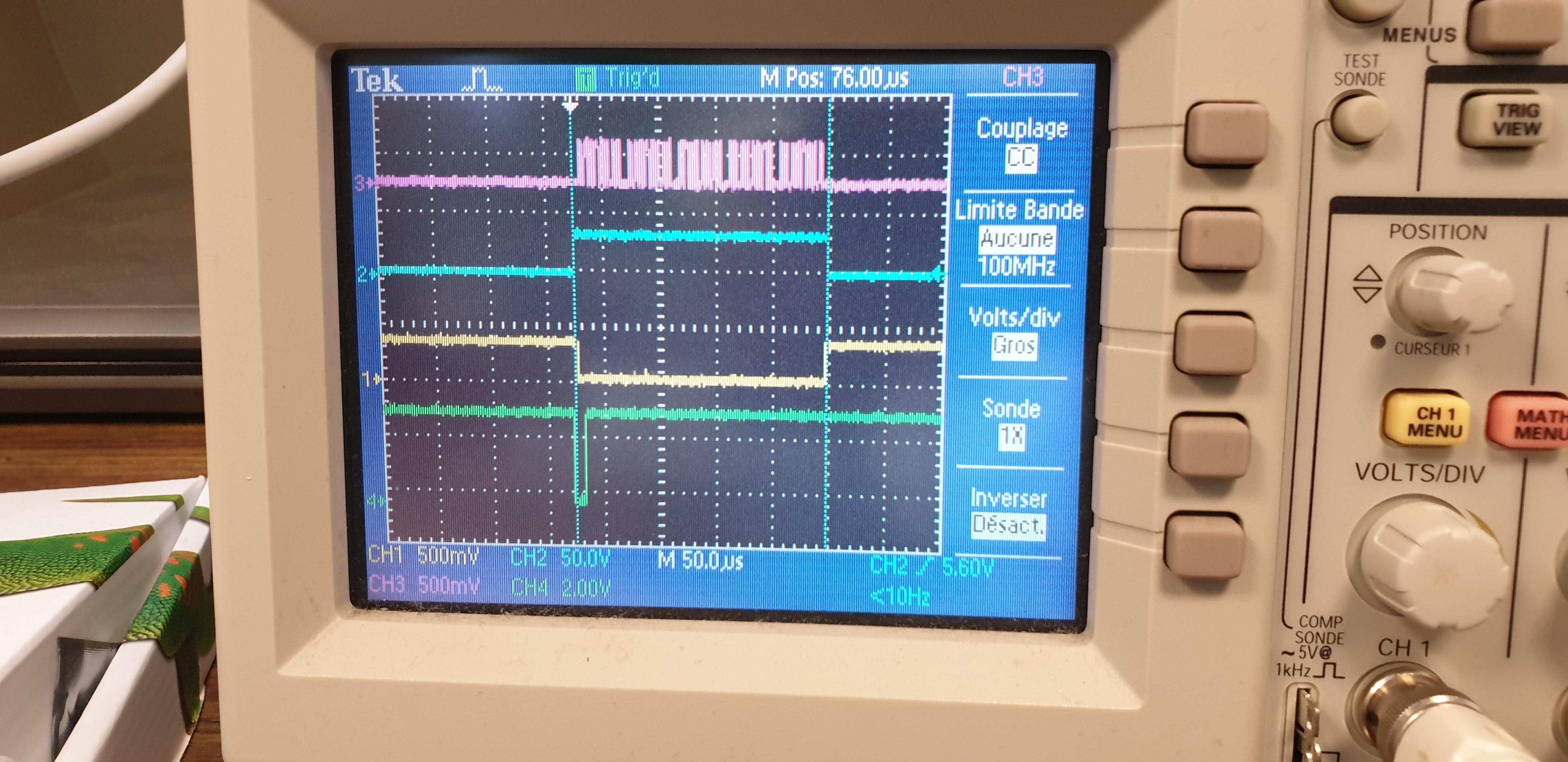
and im having some issues when i write in some registers , some of them wont change, it  gives 0 when i read them but other registers are working fine with write commande .

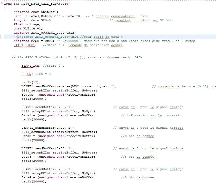
plus im having a probleme with DRDY its not working , even though  there is some signals on the input  to converte . 

i just need your help or some explanation or advices that i can maybe try it .

Thank you 

best regard 

julien 

  • Hi julien,

    We will get it back to you soon,thanks for your patience.

    Regards,

    Dale

  • Hello Julien,

    The /DRDY pin is an output that transitions low to indicate when ADC1 conversion data are ready for retrieval, the ADC is not working if a transition on /DRDY is not observed, few questions:

    1. Are you using internal oscillator, external crystal or external clock?
    2. Do you start conversion by taking START pin high or sending start1 command? continuous or one-shot conversion mode?
    3. Can you please check and confirm if your ADC device is powered properly, it's clocked, also you set the GPIOs(for reset and power-down) to the correct states in order for /DRDY to toggle and for SPI communications to work as expected?

    The command to write register(WREG) is shown in the table 37(page 85) of data sheet, also the details are explained in section WREG Command 9.5.7 section(page 87). The WREG opcode consists of two bytes. The first byte specifies the starting register address:  010r rrrr, where r rrrr is the starting register address The second opcode byte is the number of registers to write (minus one): 000n nnnn, where n nnnn is the number of registers to write minus one. The following byte (or bytes) is the register data, most significant bit first.  As a two-register write operation example shown below, the required opcodes to write data to two registers starting at register MODE2 (address = 05h) are: OPCODE 1 = 45h and OPCODE 2 = 01h. Can you please have more details about your opcodes for writing and reading the registers which are not working? 

    Regards,

    Dale

  • yes im using an internal oscillator ,and i use the Start pin , and my  ADC device is powered properly , but i didnt understand what i should do with " set theGPIOs(for reset and power-down) to the correct states in order for /DRDY to toggle and for SPI communications to work as expected" !?

    and her is a photo about my write and reading registers, and read data.

  • i want to know also the right timing or delay to use in the reading data function because it can change the values when i try different delays 

    Thank you 

  • Hi Julien,

    That will make sure the device and be reset and powered up properly, also SPI timing is correct.

    I have two questions:

    1. The different delay you mentioned is tsclk(20000) in reading data function?
    2. Which registers could you change and read successfully? which registers you could not do?

    I will look into the detail and get back to you soon, thanks.

    Regards,

    Dale

  • Hi Dale ,

    about the delay  tsclk(2000) is 2ms  , i saw many code examples and some of them are using different delays in their read data function and some are not , so i just want to know if i should put some delays in my function or not , if yes what are the good timing to put in the read data function .

    about the registers, i can change only the following registers: POWER  ,INTERFACE , MODE0, MODE1, MODE2 , INPMUX  , the others i cant . 

    Thnak you ,

    Best regard 

    Julien

  • Hi Julien,

    1. For WregADS1262( ) subroutine,the /CS pin does not need to be toggles so many times. Setting it low at the beginning of the SPI frame and high at the end of the frame should be sufficient. Also, I do not understand your purpose to use reverse().

    2. In RregADS1262( ) subroutine, I do not understand your reverse(). Also, you may need to call SPI1_setupRXInt() BEFORE you call USART1_sendBuffer().

    3. In Read_Data_Call_Back (void) subroutine, I have same question about your reverse command byte 0x12. This is usually not necessary unless your MCU sends the LSB first.

    The ADS1262 doesn’t require any delay between bytes when sending an SPI command. Only a ~50 ns delay between when /CS goes low to the first SCLK rising edge is required. In most cases the MCU will not be able to trigger a SPI send command this quickly, in which case no call to tsclk() may be needed at all.

    Regards,

    Dale

  • hello Dale ,

    the read and write commande is working perfectly  after i  called SPI1_setupRXInt() BEFORE you call USART1_sendBuffer().

    and the reverse function is  just for little to big indian  ,  

    and  how can i provide the  ~50 ns delay between when /CS goes low to the first SCLK rising edge ?

    also i have a probleme with read data function ; i just  short circuit my 2 inputs just to measur the noise, but i  recieve always hight values on the MSB instead of zero , and even if i put some votlage on the inputs , it do the same thing  ,

    (2^32 =4294967296)  its like my ads is near to be saturated   

    mesure 0 : 4244414981   ==>   it should be 0000014981
    mesure 5 : 4244415661 ==>     it should be 0000015661 
    mesure 10 : 4244415349 ==>  ......
    mesure 15 : 4244414847
    mesure 20 : 4244415688
    mesure 25 : 4244413762
    mesure 30 : 4244415296
    mesure 35 : 4244413497
    mesure 40 : 4244413477
    mesure 45 : 4244415661
    mesure 50 : 4244416358
    mesure 55 : 4244416562
    mesure 60 : 4244414851
    mesure 65 : 4244415508
    mesure 70 : 4244413065
    mesure 75 : 4244413339
    mesure 80 : 4244414570
    mesure 85 : 4244414045
    mesure 90 : 4244415690
    mesure 95 : 4244414056

    best regards


    julien

  • Hi Julien,

    I can help answer your latest questions...

    Regarding the /CS to SCLK delay, often times the MCU latency between the GPIO and SPI TX function calls will be long enough to provide for this delay. If this is the case, then you may not need to add any additional delay. If you do decide to add an additional delay, then it would probably need to go between the GPIO_PinOutClear() and UART1_sendBuffer() function calls.

    Regarding the ADC reading error, it looks like you might be reading the correct values from the SPI bus, but perhaps when you combine the Data1, Data2, Data3, and Data4 bytes, you might be accidentally introducing some incorrect values into the 32-bit word. This type of math operation in C can be a bit tricky, so please take a look at It’s in the math: how to convert an ADC code to a voltage (part 1) or this E2E Thread (https://e2e.ti.com/support/data-converters/f/73/p/699762/2587855#2587855) for some examples on how to combine the individual bytes into a single signed 32-bit data type.

  • Hi Chris,

    i read the ADC code to voltage conversion before  ,  but what im reading here is just the 32b_ data , at first  all the  data_32b were the same  , after i tried to change the config of some registers , like ysing Chop mode and IDAC rotation ,delay conversion, magnitude current , even there is no need to use some of them , but i  just  give it a try and i actualy  recieved some  reasonable  data at the speed  of 14400 sps, but i know its not the real solution .

    this is my main ,im trying to fill a chart and then read it

    and this the 32bit data  that im reading

    (data 1 is the MSB and data 4 is the LSB)

    the 32 bits data before using chop mode then idac rotation and delay conv...... like  i daid before

    mesure 0 : 9FD4FEF7
    mesure 5 : 9FD4FEF7
    mesure 10 : 9FD4FEF7
    mesure 15 : 9FD4FEF7
    mesure 20 : 9FD4FEF7
    mesure 25 : 9FD4FEF7
    mesure 30 : 9FD4FEF7
    mesure 35 : 9FD4FEF7
    mesure 40 : 9FD4FEF7
    mesure 45 : 9FD4FEF7
    mesure 50 : 9FD4FEF7
    mesure 55 : 9FD4FEF7
    mesure 60 : 9FD4FEF7
    mesure 65 : 9FD4FEF7
    mesure 70 : 9FD4FEF7
    mesure 75 : 9FD4FEF7
    mesure 80 : 9FD4FEF7
    mesure 85 : 9FD4FEF7
    mesure 90 : 9FD4FEF7
    mesure 95 : 9FD4FEF7

    then after some changes in reg config i could see some changes ,

    Read_ADC1
    mesure 0 : 09A09847
    mesure 5 : 09A09847
    mesure 10 : 09A09847
    mesure 15 : 09A09847
    mesure 20 : 09A09847
    mesure 25 : 09A09847
    mesure 30 : 09A09847
    mesure 35 : 09A09847
    mesure 40 : 09A09847
    mesure 45 : 09A09847
    mesure 50 : 09A09847
    mesure 55 : 09A09847
    mesure 60 : 09A09847
    mesure 65 : 09A09847
    mesure 70 : 09A09847
    mesure 75 : 09A09847
    mesure 80 : 09A09847
    mesure 85 : 09A09847
    mesure 90 : 49A0988F
    mesure 95 : 49A09869
     Lecture_Donnee
    mesure 0 : A09847A6
    mesure 5 : A09847A6
    mesure 10 : A09847A6
    mesure 15 : A09847A6
    mesure 20 : A09847A6
    mesure 25 : A09847A6
    mesure 30 : A09847A6
    mesure 35 : A09847A6
    mesure 40 : A09847A6
    mesure 45 : A09847A6
    mesure 50 : A09847A6
    mesure 55 : A09847A6
    mesure 60 : A09847A6
    mesure 65 : A09847A6
    mesure 70 : A09847A6
    mesure 75 : A09847A6
    mesure 80 : A09847A6
    mesure 85 : A09847A6
    mesure 90 : 00000000
    mesure 95 : A098691C

    then  it was like this

    mesure 0 : A0989F17
    mesure 5 : A0989F17
    mesure 10 : A0989F17
    mesure 15 : A0989F17
    mesure 20 : A0989F17
    mesure 25 : A098A0B0
    mesure 30 : A098A0B0
    mesure 35 : A098A0B0
    mesure 40 : A098A0B0
    mesure 45 : A098A0B0
    mesure 50 : A098A0B0
    mesure 55 : A098A0B0
    mesure 60 : A098A0B0
    mesure 65 : 00000000
    mesure 70 : A098C35E
    mesure 75 : A098C35E
    mesure 80 : A098C35E
    mesure 85 : A098C35E
    mesure 90 : A098C35E
    mesure 95 : A098C35E

    after i used the idac rotation on the hight speed 14400 , i recieved a data that are really  changing evry time and representing the noise  ,(here  i just eading  in decimale)

    mesure 0 : 4244414981  
    mesure 5 : 4244415661
    mesure 10 : 4244415349
    mesure 15 : 4244414847
    mesure 20 : 4244415688
    mesure 25 : 4244413762
    mesure 30 : 4244415296
    mesure 35 : 4244413497
    mesure 40 : 4244413477
    mesure 45 : 4244415661
    mesure 50 : 4244416358
    mesure 55 : 4244416562
    mesure 60 : 4244414851
    mesure 65 : 4244415508
    mesure 70 : 4244413065
    mesure 75 : 4244413339
    mesure 80 : 4244414570
    mesure 85 : 4244414045
    mesure 90 : 4244415690
    mesure 95 : 4244414056

    and i know that im missing something , i dont know what is it , if you could help me with it i'll appreciate it 

    thank you ,

    Best regards ,

    Julien

  • Hi Julien,

    Unfortunately, the images didn't make it through. Would you be able to resend them?

    Also, I'd be glad to review your section of code that combines the Data1-4 bytes into a 32-bit word. 

  • Hi Chris ,

    this my reaad data

    thats my main ,

    thank you ,

    Best regards,

    Julien

  • Hi Julien,

    I think you may need to include some data type casting when combining the Data1-4 bytes, specifically before the bit-shift operation. Left shifting a 8-bit value doesn't always result in values greater than 0xFF (depending on the C compiler). Therefore, make sure you cast the data to an int32_t and then perform the bit-shift operation, as in my second example:

    // Copyright (c) 2018 Texas Instruments Incorporated
    
    // Example read data function
    int32_t readData()
    {
        uint8_t ADC_data[3];
    
        // INSERT SPI COMMUNICATION HERE
        // Collect data in ADC_data array
        // where ADC_data[0] holds the MSB
        // and ADC_data[2] holds the LSB
    
        /* Return the 32-bit sign-extended conversion result */
        int32_t signByte;
        if (ADC_data[0] & 0x80u)    { signByte = 0xFF000000; }
        else                                     { signByte = 0x00000000; }
    
        int32_t upperByte   = ((int32_t) ADC_data[0] & 0xFF) << 16;
        int32_t middleByte  = ((int32_t) ADC_data[1] & 0xFF) << 8;
        int32_t lowerByte   = ((int32_t) ADC_data[2] & 0xFF) << 0;
    
        return (signByte | upperByte | middleByte | lowerByte);
    }

    Also, have you tried calling SPI1_setupRXInt() before USART1_sendBuffer() in the readData() function?

    Finally, you will probably also need to account for the timing of when your read the ADC data. Reading data in while loop will likely return many repeat conversion results, since the ADC only updates it data after the /DRDY pin signal goes low. Generally, you wait for a /DRDY falling-edge interrupt (or poll /DRDY until it read low) and then clock out the data.  

  • Hi Chris ,

    i tried the data casting and  calling SPI1_setupRXInt() before USART1_sendBuffer() in the readData() function, nothing change ,

    and what about the fact that im near to saturation , i always recieve data  near to 2^32 ,

    when my 2 inputs are in the air (not connected ) i receive these datas :

    43638
    31006
    54960
    52235
    30409
    25708
    39771
    39869
    27657
    49305
    54421
    35902
    33351
    46101
    32389
    18980
    47012
    75644
    17317
    64235
    43638
    31006
    54960

    52235

    and whenever i connect the 2 inputs together to measure the noise or even with a voltage, or if i touch the tow inputs with my hands , my values jump directly to 4200000000

    mesure 0 : 4244414981  
    mesure 5 : 4244415661
    mesure 10 : 4244415349
    mesure 15 : 4244414847
    mesure 20 : 4244415688
    mesure 25 : 4244413762
    mesure 30 : 4244415296
    mesure 35 : 4244413497
    mesure 40 : 4244413477
    mesure 45 : 4244415661
    mesure 50 : 4244416358
    mesure 55 : 4244416562
    mesure 60 : 4244414851
    mesure 65 : 4244415508
    mesure 70 : 4244413065
    mesure 75 : 4244413339
    mesure 80 : 4244414570
    mesure 85 : 4244414045
    mesure 90 : 4244415690
    mesure 95 : 4244414056

    (here my data are changing well, because i tried the idac rotation and  current magnetude and delay conversion even even there is no need to use some of them) but without them i keep recieve the same data .

    so my first probleme is : i recieve the same data without all those configurations

    second problem : im always  too near to 2^32 ,

    Best regards,

    Julien

  • Hi Julien,

    It think to troubleshoot this issue you'll need to...

    1) Set the input voltage to some known value. With the inputs floating there is really no guarantee of what you'll measure. Shorting the inputs is a good idea, just make sure to short them to a valid common-mode voltage (such as REFOUT).

    2) Look at the SPI signals on an oscilloscope or logic analyzer to see what data is coming out of the ADC. This can help you determine if the issue is in the SPI communication, or the code that is post-processing the data after you've read. If you're able to capture some screenshots of this communication, feel free to share them with us and we can help you determine if the SPI communication looks okay.

    Also, to help us help you better, would it be possible for you to share a schematic of your circuit?
    Feel free to email it to pa_deltasigma_apps@ti.com if you prefer not posting it to the forums.

  • Hi Chris ,

    i sent you a mail with the schmeatics.

    but i forgot to send you   the SPI signals on an oscilloscope ,

    Pink  sclk, yellow chip select ,green DRDY, bleu is just an I/O mesuring the time of my DRDY interruption .

    Thank you Best regards 

  • the pink are the data , i always recieve 00 on the MSB even if im on maximum 2.5

    Best regards 

    Julien